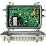
Introduction to Telecom PCB
Printed Circuit Boards (PCBs) are the backbone of modern electronics, and the telecommunications industry is no exception. Telecom PCBs are specially designed and manufactured to meet the stringent requirements of the telecommunications sector, ensuring reliable and efficient data transmission across vast networks. In this comprehensive article, we will delve into the world of Telecom PCB assembly, exploring its unique characteristics, manufacturing processes, and the challenges faced by the industry.
Key Characteristics of Telecom PCBs
High Frequency and High-Speed Design
Telecom PCBs are designed to handle high-frequency signals and high-speed data transmission. To achieve this, they require special considerations in terms of material selection, trace routing, and impedance matching. Some of the key characteristics of high-frequency and high-speed Telecom PCBs include:
- Use of low-loss dielectric materials such as Rogers RO4000 series or Isola IS400
- Controlled impedance traces to maintain signal integrity
- Careful placement of components to minimize crosstalk and signal reflections
- Use of differential pair routing for high-speed digital signals
Rigid-Flex PCBs in Telecommunications
Rigid-Flex PCBs combine the benefits of both rigid and flexible PCBs, making them an ideal choice for many telecommunications applications. These PCBs consist of rigid sections connected by flexible interconnects, allowing for three-dimensional packaging and improved reliability. Some advantages of using Rigid-Flex PCBs in telecom include:
- Reduced size and weight compared to traditional rigid PCBs
- Improved signal integrity due to shorter interconnects
- Enhanced mechanical stability and shock resistance
- Increased design flexibility for complex telecom equipment
High Layer Count and Density
Telecom PCBs often require a high number of layers and dense component placement to accommodate the complex circuitry and functionality needed in modern telecommunications equipment. High layer count PCBs can have up to 40 or more layers, enabling designers to route signals efficiently and minimize crosstalk. High-density PCBs allow for more components to be placed in a smaller area, reducing the overall size of the device.

Telecom PCB Manufacturing Process
Material Selection
Choosing the right materials is crucial for the performance and reliability of Telecom PCBs. The most common base materials used in Telecom PCB manufacturing are:
- FR-4: A glass-reinforced epoxy laminate, FR-4 is the most widely used base material for PCBs. It offers good thermal and mechanical stability, making it suitable for a wide range of telecom applications.
- Rogers: Rogers materials, such as RO4000 series, are designed for high-frequency applications. They offer low dielectric loss and stable electrical properties, making them ideal for RF and microwave circuits in telecom equipment.
- PTFE: Polytetrafluoroethylene (PTFE) laminates, such as Rogers RT/duroid, are used in high-frequency and high-speed applications due to their excellent dielectric properties and low loss tangent.
PCB Stackup Design
The PCB stackup refers to the arrangement of copper layers and dielectric materials within the PCB. A well-designed stackup ensures proper signal integrity, power distribution, and mechanical stability. In Telecom PCBs, the stackup design must take into account the specific requirements of high-frequency and high-speed signals. Some key considerations in Telecom PCB stackup design include:
- Proper placement of signal, ground, and power layers to minimize crosstalk and improve signal integrity
- Use of shielding layers to reduce electromagnetic interference (EMI)
- Balanced copper distribution to prevent warping and ensure flatness
- Selection of appropriate dielectric materials and thicknesses to control impedance and reduce signal loss
Fabrication Techniques
Telecom PCB fabrication involves a series of processes that transform the designed layout into a physical board. The main steps in Telecom PCB fabrication include:
- Imaging: The PCB layout is transferred onto photoresist-coated copper layers using UV light exposure.
- Etching: Unwanted copper is removed using a chemical etching process, leaving behind the desired copper traces and pads.
- Lamination: The individual layers are aligned and bonded together under high pressure and temperature to form a multi-layer PCB.
- Drilling: Holes are drilled through the PCB to accommodate through-hole components and vias.
- Plating: Copper is deposited onto the drilled holes and exposed copper surfaces to ensure electrical connectivity between layers.
- Solder Mask Application: A protective solder mask is applied to the PCB surface, exposing only the areas intended for component soldering.
- Surface Finish: A surface finish, such as HASL, ENIG, or Immersion Silver, is applied to the exposed copper to prevent oxidation and improve solderability.
Automated Optical Inspection (AOI)
Automated Optical Inspection (AOI) is a crucial step in the Telecom PCB manufacturing process. AOI systems use high-resolution cameras and advanced image processing algorithms to detect defects and anomalies on the PCB surface. Some common defects detected by AOI include:
- Shorts and opens in copper traces
- Missing or misaligned components
- Solder bridging or insufficient solder
- Damaged or lifted pads
By catching these defects early in the manufacturing process, AOI helps reduce the risk of costly rework and improves the overall quality of the final product.

Telecom PCB Assembly
Surface Mount Technology (SMT)
Surface Mount Technology (SMT) is the most common method used for assembling components onto Telecom PCBs. SMT involves placing components directly onto the PCB surface and soldering them in place using a reflow oven. The main advantages of SMT over through-hole technology include:
- Increased component density and smaller PCB sizes
- Faster assembly speeds and higher throughput
- Improved signal integrity due to shorter lead lengths
- Lower production costs for high-volume manufacturing
Wave Soldering for Through-Hole Components
Despite the dominance of SMT, some Telecom PCBs still require through-hole components for certain applications. Wave soldering is the preferred method for soldering through-hole components onto the PCB. In this process, the PCB is passed over a molten solder wave, which fills the through-holes and creates a reliable electrical and mechanical connection between the component leads and the PCB.
Conformal Coating
Conformal coating is a protective layer applied to the assembled PCB to shield it from environmental factors such as moisture, dust, and chemicals. In Telecom PCBs, conformal coating is especially important due to the harsh operating conditions and the need for long-term reliability. Common conformal coating materials include:
- Acrylic: Offers good moisture and fungus resistance, easy to apply and repair
- Silicone: Provides excellent temperature and vibration resistance, but can be difficult to rework
- Urethane: Offers superior chemical and abrasion resistance, but may require a longer curing time
- Parylene: Provides a thin, uniform coating with excellent dielectric properties, but requires specialized application equipment

Challenges in Telecom PCB Assembly
Signal Integrity
Maintaining signal integrity is one of the biggest challenges in Telecom PCB assembly. As data rates continue to increase and signal frequencies rise, the risk of signal degradation, crosstalk, and EMI becomes more significant. To mitigate these issues, Telecom PCB Designers must carefully consider factors such as trace routing, impedance matching, and shielding. Some strategies for improving signal integrity include:
- Use of controlled impedance traces and differential pair routing
- Proper termination and matching of transmission lines
- Minimizing crosstalk through careful component placement and layer stackup design
- Incorporating shielding layers and ground planes to reduce EMI
Thermal Management
Telecom PCBs often have to dissipate significant amounts of heat generated by high-power components such as power amplifiers, FPGAs, and processors. Effective thermal management is essential to ensure the long-term reliability and performance of the PCB assembly. Some common thermal management techniques used in Telecom PCBs include:
- Use of thermal vias to transfer heat from components to the PCB’s internal copper layers
- Incorporation of heatsinks and heat spreaders to dissipate heat away from critical components
- Design of thermal relief patterns in the PCB layout to prevent solder joint failure due to thermal stress
- Use of thermally conductive materials, such as metal-core PCBs or thermal interface materials (TIMs)
Miniaturization and High Density
The trend towards smaller, more compact telecom equipment drives the need for miniaturization and high-density PCB assembly. As component sizes shrink and pin counts increase, the challenge of achieving reliable and efficient assembly becomes more significant. Some strategies for addressing these challenges include:
- Use of fine-pitch components and high-density interconnect (HDI) PCB technology
- Adoption of advanced packaging techniques, such as chip-scale packaging (CSP) and ball grid arrays (BGAs)
- Implementation of 3D packaging and Rigid-Flex PCBs to maximize space utilization
- Use of precise and high-speed assembly equipment, such as multi-head pick-and-place machines and high-resolution inspection systems
Reliability and Testing
Ensuring the reliability of Telecom PCB assemblies is critical for maintaining network uptime and minimizing service interruptions. Comprehensive testing and quality control measures are essential throughout the assembly process to identify and address potential issues. Some key aspects of reliability and testing in Telecom PCB assembly include:
- Performing in-circuit testing (ICT) to verify the correct placement and functionality of components
- Conducting boundary scan testing to diagnose faults in complex digital circuits
- Utilizing flying probe testing for high-mix, low-volume assemblies or prototypes
- Implementing environmental stress testing, such as thermal cycling and vibration testing, to ensure the PCB’s long-term reliability
- Establishing a robust quality management system (QMS) to monitor and control the assembly process
Future Trends in Telecom PCB Assembly
5G and Beyond
The deployment of 5G networks is driving significant changes in Telecom PCB assembly. As 5G systems operate at higher frequencies and require more bandwidth, PCB designers must adapt to new materials, technologies, and assembly techniques. Some key trends in 5G PCB assembly include:
- Increased use of high-frequency laminates, such as Rogers and PTFE materials
- Adoption of advanced antenna designs, such as phased array antennas and massive MIMO systems
- Integration of active components, such as power amplifiers and switches, directly onto the PCB
- Development of novel packaging solutions, such as antenna-in-package (AiP) and system-in-package (SiP) modules
Looking beyond 5G, the industry is already exploring the potential of 6G and other advanced wireless technologies. As data rates and frequencies continue to increase, Telecom PCB assembly will need to evolve to meet the demands of these next-generation networks.
Sustainable and Eco-Friendly Practices
As environmental concerns grow, the Telecom PCB assembly industry is increasingly focusing on sustainable and eco-friendly practices. Some key initiatives in this area include:
- Adoption of lead-free and halogen-free materials to reduce the use of hazardous substances
- Implementation of green manufacturing processes, such as low-temperature soldering and VOC-free cleaning
- Use of recyclable and biodegradable packaging materials
- Incorporation of design for environment (DfE) principles to facilitate PCB recycling and disposal
By embracing sustainable practices, the Telecom PCB assembly industry can reduce its environmental impact while meeting the growing demand for eco-friendly products.
Conclusion
Telecom PCB assembly is a complex and challenging field that plays a critical role in the development and deployment of modern telecommunications networks. By understanding the unique characteristics, manufacturing processes, and challenges associated with Telecom PCBs, designers and manufacturers can create high-performance, reliable, and cost-effective assemblies that meet the ever-increasing demands of the industry.
As new technologies and trends emerge, such as 5G, miniaturization, and sustainable practices, the Telecom PCB assembly industry must continue to adapt and innovate. By staying at the forefront of these developments and embracing new materials, technologies, and processes, the industry can support the growth and evolution of telecommunications networks for years to come.
Frequently Asked Questions (FAQ)
1. What is the difference between a Telecom PCB and a regular PCB?
Telecom PCBs are specifically designed to meet the unique requirements of telecommunications applications, such as high-frequency operation, high-speed data transmission, and harsh environmental conditions. They often incorporate specialized materials, technologies, and assembly techniques that differentiate them from regular PCBs used in other industries.
2. Why are controlled impedance traces important in Telecom PCBs?
Controlled impedance traces are essential in Telecom PCBs to maintain signal integrity and minimize reflections and distortions. By carefully designing the trace geometry and dielectric properties, engineers can ensure that the impedance of the traces matches the impedance of the connected components and transmission lines, reducing signal degradation and improving overall system performance.
3. What are the advantages of using Rigid-Flex PCBs in telecom applications?
Rigid-Flex PCBs offer several advantages in telecom applications, including reduced size and weight, improved signal integrity, enhanced mechanical stability, and increased design flexibility. By combining rigid and flexible sections, Rigid-Flex PCBs enable three-dimensional packaging and can withstand the stresses and vibrations commonly encountered in telecom equipment.
4. How does Automated Optical Inspection (AOI) improve the quality of Telecom PCB assemblies?
Automated Optical Inspection (AOI) systems use high-resolution cameras and advanced image processing algorithms to detect defects and anomalies on the PCB surface, such as shorts, opens, missing components, and solder issues. By catching these defects early in the manufacturing process, AOI helps reduce the risk of costly rework, improves the overall quality of the final product, and ensures the reliability of Telecom PCB assemblies.
5. What are some of the key challenges in assembling high-density Telecom PCBs?
Assembling high-density Telecom PCBs presents several challenges, including maintaining signal integrity, ensuring proper thermal management, and achieving reliable and efficient assembly. To address these challenges, designers and manufacturers must employ advanced technologies and techniques, such as HDI PCBs, fine-pitch components, precise assembly equipment, and comprehensive testing and quality control measures.


