Introduction
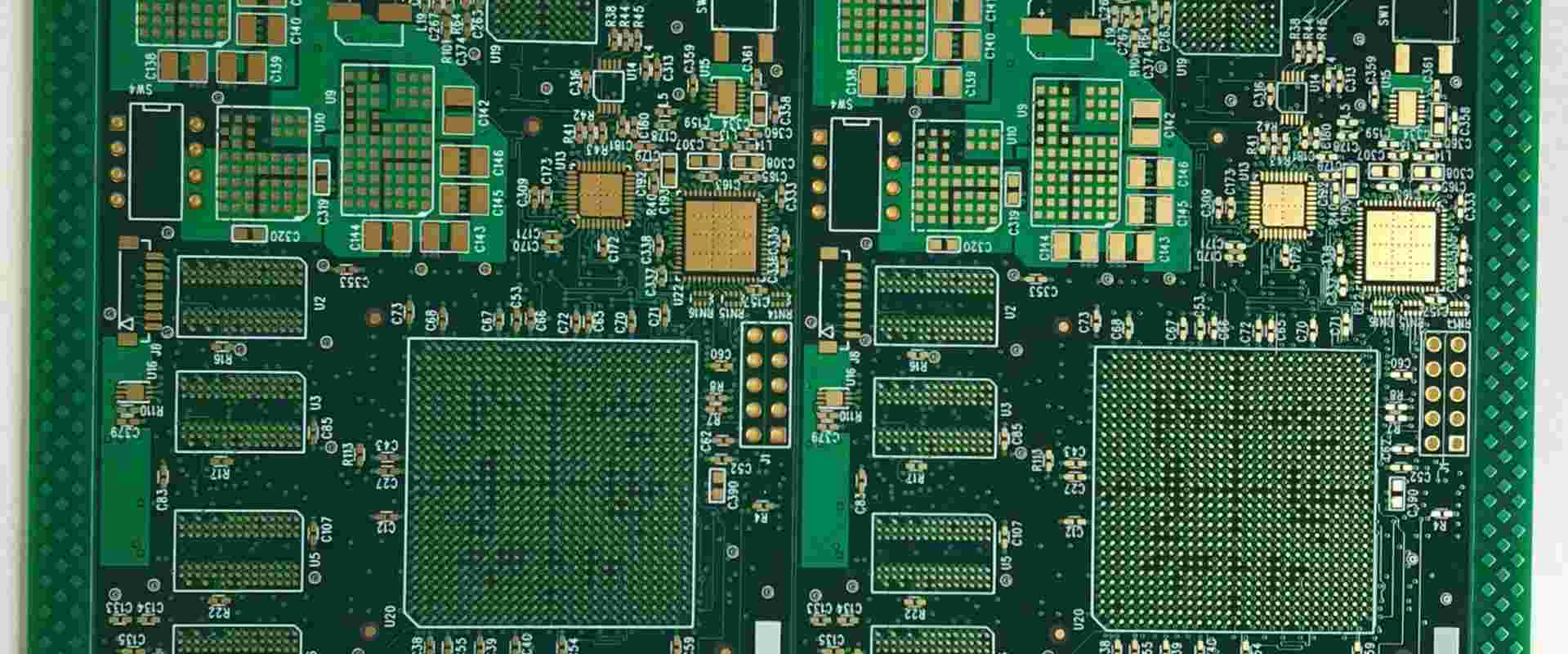
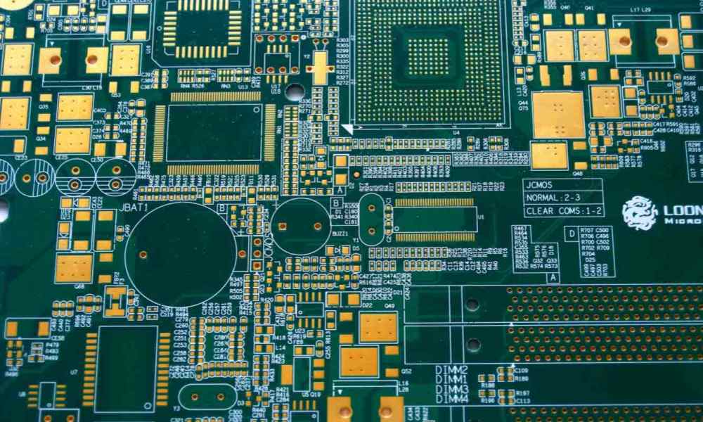
A multilayer printed circuit board (PCB) is a complex PCB structure consisting of three or more conductive layer laminations interconnected using plated through holes called vias. Compared to single or double sided PCBs, multilayer PCBs enable higher component densities by allowing more interconnections between components in different layers. They are essential for designing high performance, compact and reliable electronic circuits and systems.
This article provides a comprehensive overview of multilayer PCB technology covering the definition, properties, manufacturing processes, design considerations, applications and cost analysis of multilayer PCBs.
What is a Multilayer PCB?
A multilayer PCB is constructed by laminating multiple thin layers of circuitry bonded together using heat and adhesive pressure. The conductive layers are separated by insulating dielectric materials. Here are some key characteristics of multilayer PCBs:
- They contain 3 or more conductive copper layers separated by dielectric substrates.
- Layers are interconnected by plated through holes called vias.
- Inner layers are used to carry signals and power, outer layers for components.
- Allows packing more circuitry in a confined space.
- Enables complex circuit routing between layers.
- Provides electromagnetic interference (EMI) shielding.
- Multilayer PCBs are double-sided or multilayer boards that have been laminated together into a monolithic stackup.
- Maximum of 60-70 layers are possible with current PCB technology.
- Used in computers, communication systems, industrial equipment, automotive electronics etc.
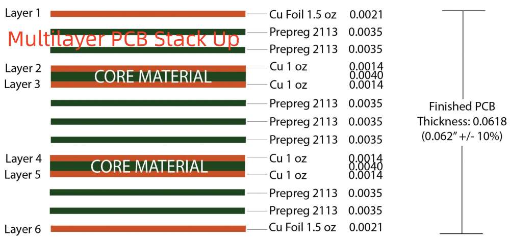
The cross-section diagram below illustrates the layer structure in a typical multilayer PCB:<img src=”https://imgur.com/R3Fr3BC.png” width=”500″ alt=”Multilayer PCB Cross Section”>
Why Use Multilayer PCBs?
Here are the main advantages of using multilayer PCBs versus single or double layer boards:
- Higher component density – Multiple layers allow fitting more components and circuitry in a compact space. This enables miniaturization.
- Complex interconnections – Routing between components on inner layers enables highly complex circuit designs.
- Signal integrity – Careful routing preserves signal integrity by preventing crosstalk and interference.
- Lower weight – More compact than using discrete PCBs or wiring harnesses for interconnections.
- EMI shielding – Ground planes between layers isolate noise sensitive signals.
- Modularity – Different functions can be separated onto specific layers.
- Better power distribution – Dedicated power/ground planes deliver cleaner power.
- Heat dissipation – Inner layers can assist in heat conduction.
Multilayer PCBs are indispensable for packing higher densities of digital circuits requiring massive interconnections that cannot be routed using less number of layers.
Properties of Multilayer PCBs
The properties of multilayer PCBs are determined by the choice of materials used and the lamination process parameters. Here are some key characteristics:
- Number of layers – As mentioned earlier, multilayer PCBs contain 3 or more conductive copper layers. Some have well over 50 layers.
- Dielectric materials – Popular dielectric substrates are FR-4, polyimide, PTFE, ceramic etc. Dielectrics provide electrical insulation between conductor layers.
- Dielectric thickness – Standard PCB dielectrics range from 0.05 mm to 1.5 mm thickness. Thinner dielectrics allow finer lines and spaces.
- Conductor thickness – Copper thickness in multilayer PCBs range from 8 μm to 105 μm. Thicker copper is used for high current carrying capacity.
- Track width/spacing – This denotes the width and spacing between adjacent copper tracks. Values range from >100 μm down to 5 μm for high density multilayer HDI PCBs.
- Number of vias – Multilayer PCBs can have from a few hundreds to over a million plated through hole vias depending on complexity.
- Finish – Multilayer PCBs employ soldermask, silkscreen, gold plating, immersion silver, OSP or other finishes.
<img src=”https://i.imgur.com/lr4zTQH.png” width=”500″ alt=”Multilayer PCB Properties”>
Manufacturing Process of Multilayer PCBs
Fabricating multilayer PCBs involves complex processes and requires advanced equipment. The typical manufacturing steps are:
1. Inner Layer Preparation
- Flame retardant glass fabric reinforcement like FR-4 is impregnated with resin to create dielectric core.
- Copper foil is laminated to one or both sides of dielectric to form a copper clad laminate.
- Photoresist dry film is applied on copper layers and circuit patterns are imaged using lithography process.
- Exposed copper without photoresist is etched away chemically leaving desired inner layer traces.
2. Lay Up
- Etched inner layers are inspected and prepared for stacking.
- Layers are arranged in a sandwich with dielectric prepregs between each foil-etched core.
- Alignment accuracy is critical especially for fine line HDI boards.
- Lay up thickness depends on number of layers.
3. Lamination
- The multilayer PCB layer stackup is vacuum pressed at high temperature allowing resin flow and bonding.
- Pressure, temperature and time parameters are controlled for adhesion.
- Some PCBs use teflon/polyimide dielectrics requiring higher lamination temperature.
4. Via Drilling
- Small holes are precision drilled through the laminated stackup to interconnect all layers.
- Excellent drill location accuracy is required to avoid hitting inner traces.
- Drilling is done using small twist drills or laser/plasma processes.
5. Plating
- Walls of through holes are plated with copper electrolessly followed by electrolytic copper.
- Plating makes the vias conductive between layers.
- Plating controls hole wall roughness and copper thickness.
6. Outer Layer Processing
- Similar to inner layers, outer layer circuits are lithographically etched on both outer surfaces.
- Additional finishing steps like soldermask, silkscreen printing, surface finishes are done.
7. Testing
- Completed multilayer PCBs undergo electrical testing (ICT) and AOI inspection before shipment.
- Testing checks for shorts, opens, impedance etc.
This video illustrates the multilayer PCB fabrication process:
Design Guidelines for Multilayer PCBs
To leverage the full benefits of multilayer PCB technology, designers need to follow certain guidelines:
- Layer stack planning – Proper sequence placement of signal, ground and power layers. Avoid adjacent power/ground layers.
- Bypass capacitors – Use sufficient bypass/decoupling caps for each IC near signal vias. Filters noise on power distribution.
- Controlled impedance – Match trace impedance to source/load impedance. Use impedance calculators.
- Minimize vias – Many vias can cause reflection and signal loss at higher frequencies. Use direct routes.
- EMI control – Use ground/power planes between critical signals. Provide proper board shielding.
- Thermal design – Ensure vias and layers distribute heat efficiently from hot components.
- High speed traces – Minimize length deviations/stubs for clock and fast data signals.
- Component placement – Optimize placement to minimize track lengths and allow easier routing.
- Stackup symmetry – Maintain same stackup sequence from center for mechanical stability.
Applications of Multilayer PCBs
Some major application areas where multilayer PCBs provide benefits are:
- Computers – Motherboards, display cards, hard disk drive controllers with high speed digital processors and massive signal routing require multilayer boards.
- Smartphones – Multilayer PCBs pack communication processors, application processors, memory, power management circuits in the compact form factor.
- Communication – Complex wired/wireless transmission systems like 5G, routers, base stations to support very high frequencies need multilayer boards.
- Automotive – Electronic control units for engine, ABS, airbags, traction control etc use multilayer boards extensively.
- Defense & Aerospace – Avionics computers, radars, guidance systems require multilayer PCBs to package density, speed and reliability.
- Industrial – Programmable controllers, process automation systems, test equipment use multilayer boards with high layer counts.
- Medical – Portable health monitors, imaging systems like MRI machines have multilayer PCBs to integrate sensors, processors and other components.
Multilayer PCB Material Options
Popular dielectric/substrate options for manufacturing multilayer PCBs include:
FR-4
- Most common, cost effective dielectric for multilayer PCBs is FR-4 glass reinforced epoxy.
- Has good mechanical properties but limited electrical performance.
- Usable for digital circuits below 5GHz like computers, consumer electronics.
High Tg FR-4
- Modified FR-4 with higher glass transition temperature (>170°C).
- Improves thermal reliability ideal for lead-free assembly.
- Often used for industrial controls, automotive electronics.
Rogers High Frequency Laminates
- PTFE based composites like RO4350, RO4003 for microwave and mmWave frequencies above 10 GHz like radars, 5G systems.
- Excellent electrical characteristics with well controlled dielectric constant and low loss.
Polyimide
- Used for flex PCBs but also as multilayer boards for high temperature and flexing applications.
- Withstands over 200°C ideal for down-hole, aerospace and defense systems.
Isola High Performance Laminates
- Isola’s laminates like 370HR, AstraMT77 allow high performance PCBs with Dk as low as 3.0 for high speed data signals.
Ceramics
- Advanced ceramic substrates like aluminum nitride or alumina provide thermal conductivity needed in high power circuits.
Examples of Multilayer PCBs
Here are some examples of multilayer PCBs used in real-world applications:
- 16-24 layer boards used in desktop and laptop motherboards with high speed processors, memory and peripherals.
- 20 layer Flex-rigid PCBs used in cell phone designs to integrate rigid and flex sections with components on both sides.
- 28 layer HDI boards for automobile engine control units packing multiple processors, memory and SMD components.
- 32 layer boards with 20μm line/space and 6mil vias made using laser drilled microvias in the latest smartphones.
- 60 layer board with 16 buried and 28 external planes at 25μm spacing used in RADAR systems.
- 10 layer 0.8mm thick metal-core PCBs used in LED luminaires to manage heat dissipation and reliability.
Multilayer PCB Manufacturers
Some of the top companies providing advanced multilayer PCB prototyping and volume production services include:
- TTM Technologies
- AT&S
- Compeq Manufacturing
- Tripod Technology
- NanYa PCB Corp
- CMK Corporation
- Unimicron
- RayMing Technology
- Würth Elektronik
- Zhen Ding Tech
These multilayer PCB manufacturers offer services on conventional, HDI and complex multilayer boards using cutting edge fabrication processes and testing. Their expertise spans across industry verticals including communications, aerospace, defense, automotive, industrial and medical electronics.
Cost Analysis of Multilayer PCBs
The manufacturing cost of multilayer PCBs depends on various factors:
Key Cost Drivers:
- Number of conductive layers
- PCB thickness
- Dielectric material type
- Layer count
- Copper thickness
- Minimum track/space
- Number of vias
- Board size
- Special finishes like gold plating
- lead-free HASL, OSP, immersion silver etc.
- Tolerances and testing
- Volume
- Special fabrication process requirements like backdrilling plated through holes
Here is a rough estimate of multilayer PCB cost based on the number of layers:
| No. of Layers | Cost per square inch |
|---|---|
| 4-6 layers | $5 – $15 |
| 8-10 layers | $10 – $25 |
| 12-16 layers | $15 – $40 |
| >18 layers | $25 – $60 |
As can be seen, cost rises exponentially as the layer count increases due to the complex lamination process steps involved.
Frequently Asked Questions
Q: How are signals routed in multilayer PCBs?
A: Signals are routed on internal layers by etching copper traces. Vias interconnect traces between layers. Sensitive signals route adjacent to ground/power planes.
Q: What are HDI multilayer PCBs?
A: HDI or High Density Interconnect PCBs have line width/spacing below 100 microns (4 mils), microvias and often employ newer materials like LCP.
Q: Can flex PCBs be multilayer?
A: Yes, flex PCBs can be fabricated using multilayer technology by alternating flexible dielectric films with adhesive and copper foils.
Q: What is the difference between multilayer and double sided PCBs?
A: Double sided PCBs have conductors on both top and bottom surfaces. Multilayer PCBs have 3 or more conductor layers interconnected internally by plated through hole vias.
Q: How are multilayer PCBs tested?
A: They undergo net connectivity checks, opens/shorts, leakage testing and other electrical inspections using flying probe testers, in-circuit test systems and automated optical inspection.


