Introduction
Printed circuit boards (PCBs) are an essential component of most electronic devices. A PCB provides the mechanical structure to support and electronically connect components using conductive tracks, pads and other features. The PCB manufacturing process transforms the design into a physical board ready for population with components.
This guide will provide a step-by-step overview of the major steps involved in manufacturing a printed circuit board from design to finished product. We will look at the key processes of materials selection, imaging, etching, lamination, drilling, plating, testing and inspection that turn design files into functional PCBs. Understanding the PCB production process helps designers, engineers and manufacturers optimize the design, select suitable materials and fabrication methods and ensure quality standards are met.
PCB Design and Layout
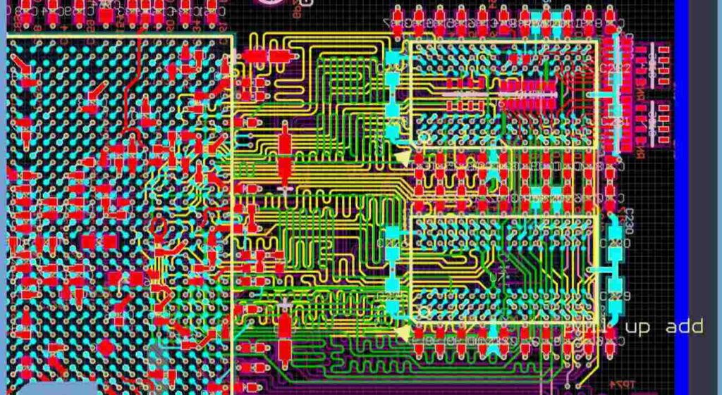
The first step in the PCB production workflow is creating the board design files. PCB layout design is usually done using Electronic Design Automation (EDA) software such as Altium, Eagle, KiCad or OrCAD. The designer will produce a set of Gerber files – the industry standard for PCB image data – that contain copper layers, solder mask, silkscreen legend, drill files and other instructions.
The PCB layout will define the number of copper layers (usually 1-16), the traces, pads, vias, holes and other features. Key considerations during layout and design include:
- Circuit density and complexity
- Component spacing, positioning and orientation
- Critical signals and controlled impedance routes
- High current traces and heat dissipation needs
- EMC, noise and crosstalk prevention
- Locations of connectors, indicators and buttons
- EPA clearance and creepage requirements
The board layers, features, materials and finishes defined in the design stage will dictate the fabrication methods required.
Materials Selection
The Gerber files provide fabrication data but the PCB manufacturer also needs to determine suitable materials for the design. Key material choices include:
Substrate
The substrate or base material is the foundational insulator layer that supports the conductive copper traces. The most common options include:
- FR-4 Glass Epoxy – Economical, flame resistant and suitable for most consumer PCBs
- High Frequency Boards – PTFE, ceramic, hydrocarbon variants for RF or high speed boards
- Metal Core Boards – Aluminum or copper substrate for high power LEDs or power electronics
Copper Foil
The conductive traces are formed from copper foil laminated onto the substrate. Common thicknesses range from 1⁄4 oz (0.7 mils) to 2 oz (70 mils). Thicker copper is used for high current applications.
Soldermask
The soldermask is the protective coating that isolates copper traces from solder and environmental corrosion. Photoimageable “dry film” and liquid photo resists are the most popular options.
Silkscreen
The silkscreen is the printed legend on the PCB that labels components, shows logos and identifies board functions. White is standard but different colors are also used.
Plating
Gold, tin, silver, nickel and other metal plating maybe applied over pads and vias to facilitate soldering and prevent oxidation.
Stiffeners
Metal stiffeners and bars may be incorporated to prevent warping and bowing of large or thin PCBs.
Imaging
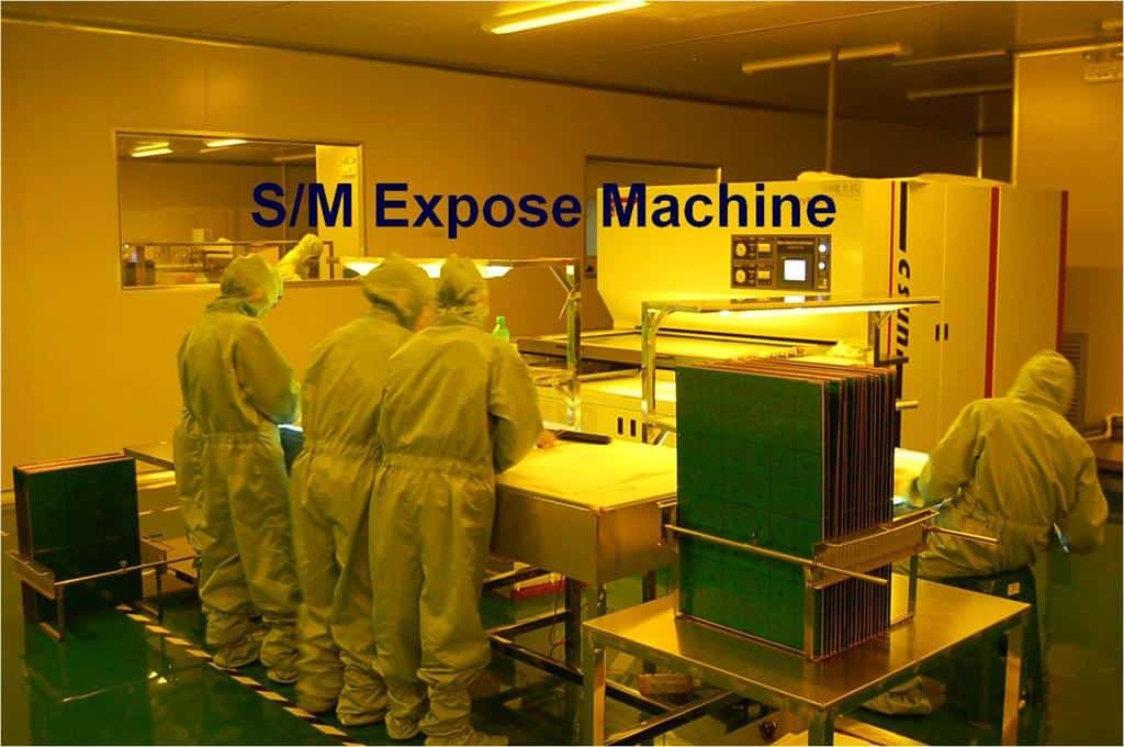
The PCB manufacturer will take the Gerber files from the customer and image or transfer the layer data onto the relevant materials using a photolithographic process.
Photoresists
Liquid photoresist material is coated onto the substrate. Two types are used:
- Positive Photoresist – Exposure to light makes it soluble. Masked areas remain once developed.
- Negative Photoresist – Exposure makes it insoluble. Exposed regions remain after development.
Phototools
Phototools contain the PCB image data as opaque and clear areas and are placed over the photoresist:
- Film Phototools – Printed transparencies with image regions defined. Inexpensive but can have resolution limits.
- Direct Imaging – Laser or maskless lithography systems ‘draw’ the image onto the photoresist. Higher resolutions but slower and more expensive.
Exposure and Development
The resist is exposed to high intensity UV light, making exposed areas soluble in developer chemicals. The unexposed resist remains, masking the material below. Photoresist patterns for conductors (plating resist) or etching (etch resist) are generated.
Clean and Prep
Surfaces are cleaned and treated to improve photoresist adhesion. A photoresist laminator can be used to apply dry film resist.
Etching

Etching removes copper from the substrate to create the conductive pattern of traces, pads and features.
Wet Chemical Etching
Liquid etchant chemicals dissolve away unwanted copper. Ferric chloride and ammonium persulfate are commonly used etchants. The etchant tank is agitated to provide fresh solution and remove etched copper.
Dry Etching
Plasma gas etches copper in a vacuum chamber. More expensive but better fine feature control and no liquid waste disposal.
Lamination
Pre-impregnated (prepreg) fiber sheets are stacked up, along with sheets of copper foil. The multilayer stack is laminated under heat and pressure to fuse the layers into a single circuit board panel.
The lamination process:
- Arranges sheets in a book for the cross section required
- Uses interleaving papers if needed between prepreg layers
- Applies high pressure to the stack at an elevated temperature
- Cures the resin which bonds the layers into a solid board panel
Drilling

The laminated board now has holes drilled at specified positions to create vias – plated through holes that connect different layers.
Mechanical Drilling
CNC drilling machines use high speed bits to precisely drill holes defined in the drill files. Excellent dimensional accuracy but limited in aspect ratio and hole size.
A laser beam ablates material to drill small holes with diameters below 150μm. Higher accuracy and speeds but more expensive.
Punching
A mechanical punch can create large holes above 0.4mm. Faster than drilling but lower precision.
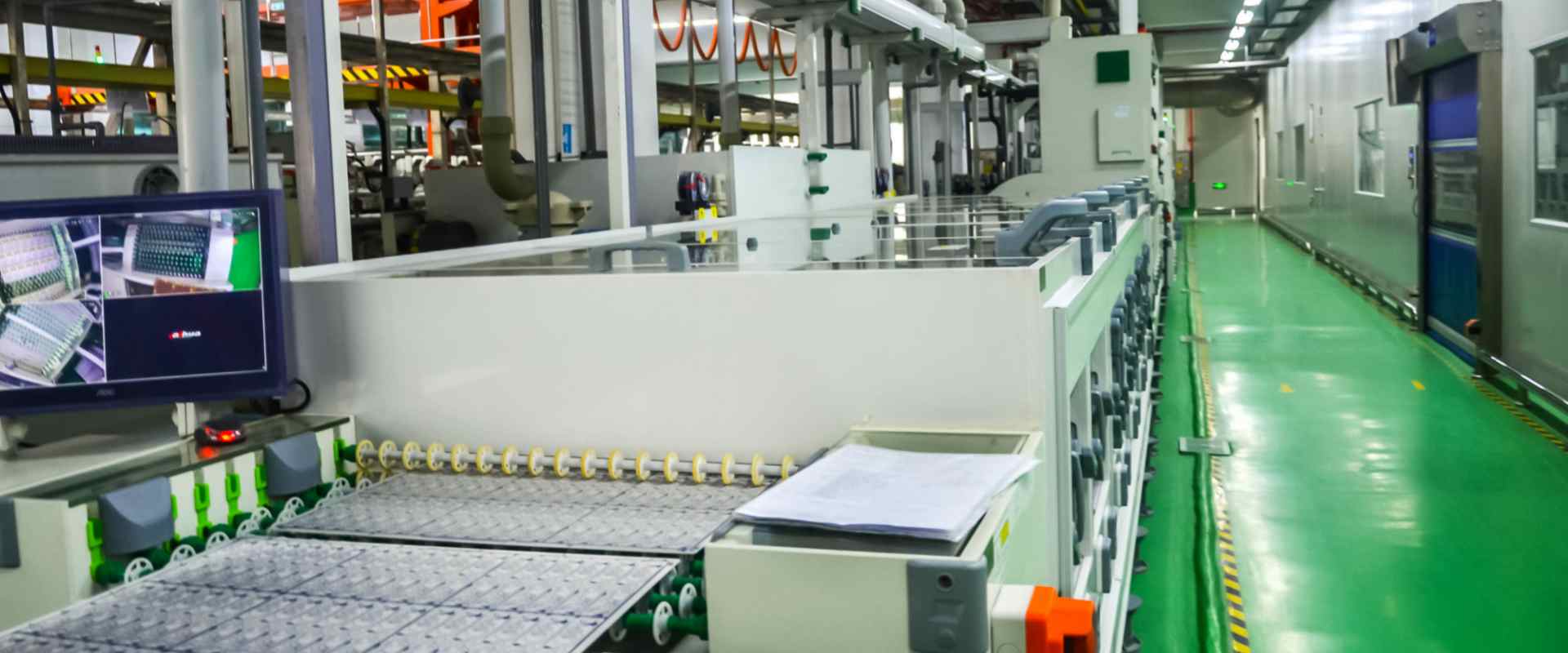
Plating and Coating

Conductive and protective coatings are applied to the panel.
Electroless Copper
An auto-catalytic chemical process uniformly deposits a thin layer of copper over the entire board to make non-conductive holes conductive.
Electrolytic Copper Plating
A thicker copper layer is plated onto conductive areas to build up trace thickness. Photoresist masks areas that will remain non-conductive.
Tin-Lead or HASL
Hot Air Solder Leveling (HASL) deposits a solder coating onto pads for solderability and corrosion protection. Being phased out due to lead.
Immersion Tin, Silver, Gold
Immersion plating deposits metals selectively only onto exposed copper regions. Provides excellent solderability while avoiding shorts.
ENEPIG (Electroless Nickel Electroless Palladium Immersion Gold)
Multistage process that deposits nickel, then palladium and finally flash gold for maximum performance and reliability.
Soldermask & Silkscreen
The soldermask insulator and component silkscreen layers are applied as explained in the materials selection stage. Openings in the soldermask define solderable regions.
Panelization
The large circuit board panel consisting of many individual boards is sectioned into the separate PCB units using a process called depanelization. Common methods include:
- V-Scoring – V shaped grooves cut into the panel along board boundaries to guide breaking
- Routing – A CNC milling machine cuts out the individual boards
- Punching – A punch die cuts the boards out of the panel
Electrical Testing

PCBs are tested to verify the board matches design specifications and functions correctly before population with components.
In-Circuit Testing
A “bed of nails” test fixture makes spring contact at test points. Each circuit is tested for opens, shorts and function.
Flying Probe Testing
Programmable probes on X-Y axes are positioned at each test node. Eliminates need for fixtures.
Boundary Scan
Serial chain of built in self test cells around each component pin are used to test interconnects between ICs.
Automated Optical Inspection
A high resolution camera captures images that are checked against a good board reference to identify any defects.
Final Finishes
Boards may receive final surface finishes and markings. These include:
Marking – Date codes, logos, identification numbers applied with inkjet or laser Permanent Soldermask – LPI soldermask for scratch protection and improved aesthetics Spot Coating – Conformal coating, polyurethane or epoxy applied onto individual components or areas for environmental protection Edge Connector Plating – Selective gold plating on edge fingers to improve durability
The finished PCBs are now ready for assembly and population with electronics components to build the desired system or product.
Summary of the PCB Manufacturing Process Workflow
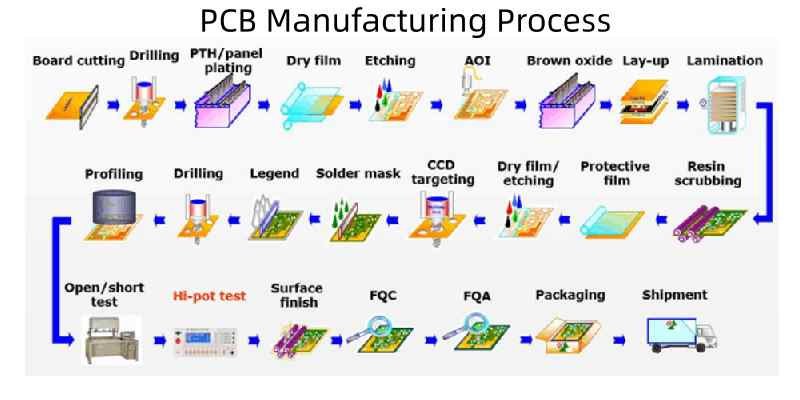
To recap, the typical sequence of production steps to convert design files into completed printed circuit boards are:
- PCB Layout Design – Generate Gerber and drill files
- Materials Selection – Match substrate, copper weights, finishes etc. to design
- Imaging – Photolithography to transfer layout onto each layer
- Etching – Remove copper to form traces and pads
- Lamination – Fuse substrate and prepreg layers under pressure and heat
- Drilling – Drill holes for component pins and vias
- Plating – Electroless then electrolytic copper deposition
- Coating – Apply solder mask and silkscreen print
- Panelization – Break panel into individual PCBs
- Testing – Validate board is defect free and functioning
- Final Finishes – Additional markings, spot coats or edge plating
Understanding this end to end fabrication process enables PCB designers and engineers to make informed design decisions and work effectively with their board manufacture partner to produce a quality printed circuit board assembly.
Frequently Asked Questions
What are some key factors to consider during PCB layout and design?
Some key considerations during layout include circuit density, high speed routing, controlled impedance, thermal management, EMC/EMI, component placement, ease of assembly, test points and manufacturability. Taking fabrication requirements into account during the design stage helps avoid issues later on.
Why is surface preparation important before coating photoresist?
Surface preparation by cleaning and roughening improves photoresist adhesion. This prevents masking layers from peeling or flaking during development which would ruin the PCB image transfer.
What are tradeoffs between mechanically drilled and laser drilled PCB holes?
Mechanical drilling can achieve very high accuracy but is limited in aspect ratios and achievable hole sizes. Laser drilling can create micro-vias below 0.15mm and high density arrays but the holes may exhibit slightly more variation.
What plating is typically used for PCB finishes?
Common plating finishes include HASL, immersion silver or tin, hard gold and ENEPIG. Key considerations are solderability, durability, shelf life, environmental performance and cost. Lead-free finishes are preferred due to environmental regulations.
How does flying probe PCB test differ from using a fixture?
Flying probe testing uses programmable pins on X-Y axes so custom fixtures are not needed. This reduces costs but may be slower than dedicated board-specific fixtures used in in-circuit testing.
What are some methods used for depanelization of a PCB array?
Common approaches are V-groove routing to guide breaking, using a CNC milling machine to precisely cut out boards or using a punch-press die to punch boards out of a panel. The method depends on the board size and features.
This covers the key steps and considerations at each stage of the printed circuit board fabrication process from layout through to finished boards. Let me know if you need any clarification or have additional questions!


