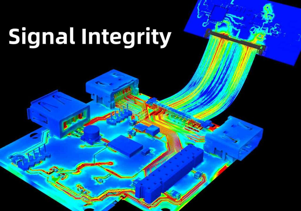
As electronics become faster with data rates exceeding Gbps speeds, ensuring flawless signal transmission across PCB interconnects proves imperative for reliable functionality. However, several parasitic electrical phenomenon during high speed signaling can accumulate degrading waveform quality – falling under the discipline of signal integrity.
This comprehensive guide covers common signal integrity issues plaguing fast digital designs including:
- Signal integrity basics
- Major threat types
- Modeling & analysis techniques
- Mitigation methods through PCB design choices
- Validation testing measures
Learning signal integrity design practices enables electronics engineers to ship robust productsresistant to signal corruption over complex boards operating at cutting edge frequencies.
Signal Integrity Introduction
Before diving into integrity threats, let’s build foundations understanding two key signal concepts:
Rise Time (Tr) – The interval for signal waveform amplitude changing from 10% to 90% threshold during switching
Bit Period (T) – The temporal duration encapsulating one complete logic bit
Tr defines signal content maximum frequency, while T corresponds to single bit rate:
As data bandwidth increases, Tr shrinks and T compresses. This stresses underlying systems obeying frequency dependant behaviors. Quantifying Tr and T for designs sets the stage assessing signal integrity readiness.
Threats arise when interacting PCB parasitics hinder fast edge behavior. We’ll survey common issues next.
Types of Signal Integrity Problems
Electrical phenomena degrading signal waveforms mainly include:
1. Reflections
Fast rising edges hitting abrupt impedance mismatches reflect energy back creating distortions. Reflections stem from uneven circuit geography.
2. Crosstalk
Adjacent signal traces capacitively or inductively couple to each other creating unintended mutual interference. Dense parallel routings increase crosstalk risks.
3. Ringing
Resonance during switching from impedance mismatches causes signal overshoot and ringing oscillations corrupting data.
4. EMI Radiation
Rapid changing currents emit electromagnetic interference (EMI) noise disrupting nearby components. Lacking current return paths fuels EMI.
5. Power Integrity Fluctuations
Noisy or unstable PCB power distribution degrades signaling through shared references coupling noise vulnerabilities.
We’ll overview analysis methods managing these signal integrity phenomenon next.
Modeling and Analysis Techniques
PCB design tools leverage various modeling techniques assessing signal integrity early in the design flow:
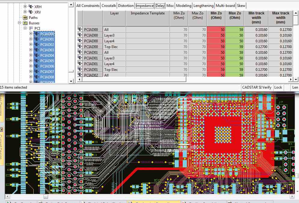
Transmission Line Modeling
Models entire path segments as distributed RLGC transmission line elements capturing frequency behavior. Applies past ~200-500 MHz speeds.
Lumped Element Modeling
Models net fragments using concentrated RLC elements making computations easier. Valid for slower signals below ~200 MHz.
Electromagnetic Analysis
Full wave 3D field solvers model high frequency wave propagation visually showing radiating and coupling EMI risks.
Power Integrity Analysis
Models DC rails with RLC grids predicting noise/ripple and voltage drop across PCB area filling gaps left by signal analysis methods.
Integrating appropriate modeling approaches matching geometric wavelengths and data-rates scale proves essential seeing issues arising later. Running simulations early in the design flow prevents extensive re-spins rectifying SI issues spotted too late downstream during prototype bring-up.
Now we’ll explore key signal integrity design guidelines improving PCB reliability.
PCB Design Guidelines Guarding Signal Integrity
Several prudent design strategies applied during layout mitigate signal integrity pitfalls:
1. Capacitive Decoupling
Sprinkling capacitors supplying charge reservoirs locally alongside high speed ICs smooths transient switching noise/ground bounce when electrically near amplifier inputs for stabilizing integrity. Values ranging 0.01-0.1uF work well.
2. Terminating Traces
Matching trace impedance to driver output and receiver input characteristics prevents problematic reflection voltage spikes from signal discontinuities using series/parallel resistor combinations.
3. Ground Plane Integration
Complete unbroken ground planes underlying signals provide current return paths mitigating inductive radiation/loops while shielding EMI infiltration into traces due to micro-coaxial effects.
4. Reduced Coupling
Maximize spacing between fast parallel traces, route orthogonally minimizing mutual length or insert ground guards for reducing capacitive/inductive crosstalk below 10-20% Vpeak thresholds.
5. Component Placement
Group associated circuits together minimizing trace lengths rather than scattering related blocks wasting routing real estate increasing parasitics exposing signals unnecessary to EMI interference risks longer.
6. Topology Techniques
Leverage daisy chains, differential signals or meander geometries for improved impedance control, electromagnetic compatibility and noise immunity essential for multi-Gbps links.
7. Stackup Optimization
Arrange signal/ground layer order, dielectric materials and thickness balancing impedance needs without manufacturability penalties enabling performance. Carefully engineer to meet bandwidths demands.
Applying these guidelines through intentional PCB stackup configurations, component placement decisions and trace routing allows meeting signal integrity while achieving manufacturability simultaneously.
We’ll cover validation processes confirming design signal integrity next.
Testing and Validation Methods
Despite extensive modeling guiding designs, physical validation across frequency spectrum proves prudent guaranteeing product performance before volume production:
Time Domain Reflectometry
Launch fast impulse evaluating reflections sniffing out discontinuities otherwise missed in frequency domain simulation limitations.
Vector Network Analysis
Sweeps bandwidth characterizing attenuation, time delays and reflection parameters suggesting stackup/termination adjustments needed through iterative empirical correlation work.
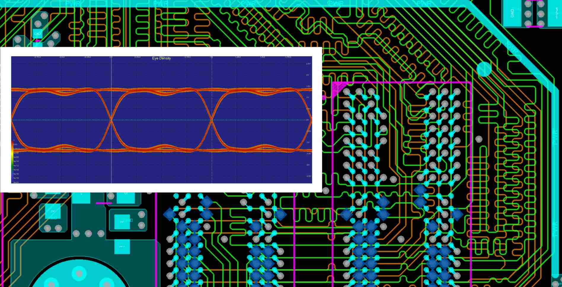
Eye Diagram Analysis
Overlays sampled waveform elucidating noise margins available inside data eye openings available for ensuring reliable digital signal detection by receivers.
Bit Error Rate Testing
Stresses signaling measuring data decision point margin statistics quantifying sensitivity towards integrity degradation applied for system robustness sign-off avoiding subtle issues slipping through initial testing.
While modeling and guidelines minimize threats, ultimate vetting through physical measurement optionally suggests refinement opportunities not fully emulated strengthening overall integrity ensuring flawless product functionality.
Now we’ll cover some frequently asked questions on the topic.
Common Signal Integrity FAQs
What are typical signal integrity analysis/testing costs?
Plan at least $5000-10000+ for extensive signal integrity analysis/physical testing which proves worthwhile preventing extensive respins late catching issues after release. Costs vary based on analysis depth needs and physical measurement equipment time required.
What PCB features help mitigate EMI specifically?
For reducing electromagnetic interference, flooded unbroken ground planes, ground vias fencing signals, multi-point component common grounding, inductance cancelling differential pair routing, transmission line techniques and minimize aperture openings all contribute towards effective EMI containment.
How are simulations correlated to actual measured results?
Engineers iteratively tweak dielectric properties, component parameters and model dimensional accuracy relative to PCB fabrication data through multiple simulation cycles until reaching agreements with impedance, time domain reflectometry and network analyzer test signature validations converging measured results.
Can microcontrollers with fast rise times function properly from low speed PCBs?
While microcontrollers may themselves support >1Gbps speeds, their integrated PCBs must provide appropriately controlled impedance links between chip pins to external channels to guarantee clean signal transmission at rated bandwidths without corruption. Speed grade matching throughout proves critical.
Are tear drop stubs required at fast logic vias?
Tear drop anti-pad stubs help control via inductance but consume additional routing channels around pads making high density escapes challenging. Evaluate necessity based on simulated ringing versus layout congestion tradeoffs for the most sensitive signals above ~5 Gbps or so.
This covers common questions around applying signal integrity analysis to enable robust PCB functionality at growing data rates.
Conclusion
In closing, mastering signal integrity through intentional design techniques, modeling simulations augmented by physical measurement proves pivotal keeping pace with bandwidth increases stressing tolerances while balancing manufacturability tradeoffs. When signals maintain integrity without corruption, electronics achieve sustainable performance across application lifetimes despite miniaturization pressures challenging electrical designs. Signal integrity mastery allows designers to confidently push envelopes releasing innovations ahead of the future.


