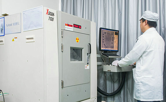
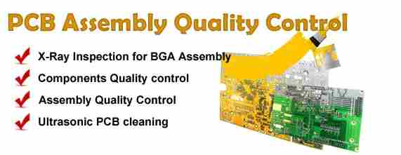
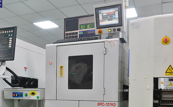
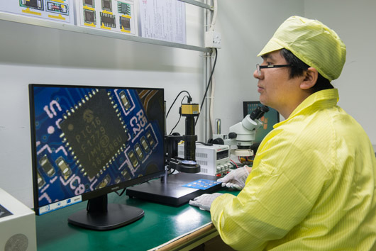
X-Ray Inspection for BGA Assembly
Our automated X-ray inspection systems are able to monitor a variety of aspects of a printed circuit board in assembly production. The inspection is done after the soldering process to monitor defects in soldering quality. Our equipment is able to”see” solder joints that are under packages such as BGAs, CSPs and FLIP chips WHERE the solder joints are hidden.
This allows us to verify that the assembly is done right. The defects and other information detected by the inspection system can be quickly analyzed and the process altered to reduce the defects and improve the quality of the final products. In this way not only are actual faults detected, but the process can be altered to reduce the fault levels on the boards coming through. Use of this equipment allows us to ensure that the highest standards are maintained in our assembly.
Components Quality control
To make sure the components to be used are good quality, there are several processes that we follow:
1. An overview of the visual electronic components inspection process includes:
* Packaging examined:
-Weighed and checked for damage
-Taping condition inspected-dented package etc.
-Original factory sealed vs. non-factory sealed
* Shipping documents verified
-Country of origin
-Purchase order and sales order numbers match
* Manufacturer P/N, quantity, date code verification, RoHS
* Moisture barrier protection verified (MSL)-vacuum sealed and humidity indicator with specification (HIC)
* Products and packaging (photographed and cataloged)
* Body marking inspection (faded markings, broken text, double print, ink stamps, etc.)
* Physical conditions inspection (lead bands, scratches, chipped edges, etc.)
* Any other visual irregularities found
Once our visual distribution inspection is completed, products are escalated to the next level-electronic components engineering distribution inspection for review.
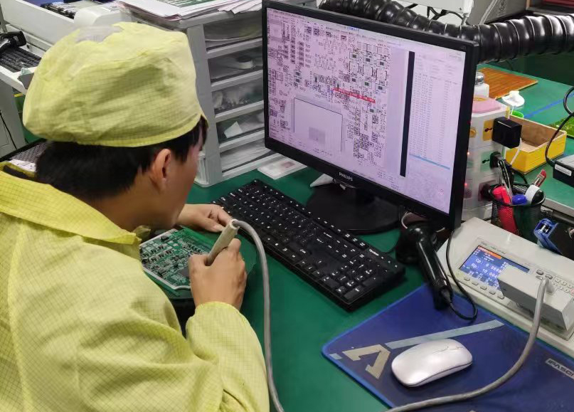
2. Engineering Components Inspection
Our highly skilled and trained engineers receive the components for evaluation at a microscopic level to ensure consistency and quality. Any suspect parts or discrepancies that are discovered in the visual inspection process will either be verified or discounted by taking a product sampling of the material/parts.
The engineering electronic components distribution inspection process includes:
* Review visual inspection findings and notes
* Purchase and sales orders numbers verified
* Verification of labels (bar codes)
* Manufacturer’s logo and date log verification
* Moisture sensitivity level (MSL) and RoHS status
* Extensive marking permanency tests
* Review and comparison to manufacturer datasheet
* Additional photos taken and cataloged
* Solderibility Testing, the samples undergo an accelerated ‘aging ‘ process before being tested for solderibility, to take into consideration the natural aging effects of storage prior to board- mounting; In addition to the Engineering Components Inspection we have a higher level of inspection under the customer request.
3. By customer request, all components can pass a thorough final inspection in our Assembly facility.
Detectable defects list
| Defect No. | Defect Description | Selected Inspection Technology(s) | Defect Class | Automated Detection by final prototype |
|---|---|---|---|---|
| 1 | Dry joints | AOI | Soldering | No |
| 4 | BGA voiding | X-ray | Soldering | Yes |
| 5 | BGA bridging | X-ray | Soldering | Yes |
| 6 | BGA tilted | X-ray | Soldering | Yes |
| 7 | BGA missing balls | X-ray | Soldering | Yes |
| 8 | BGA poor wetting | X-ray | Soldering | Not reliable detection |
| 9 | BGA poor reflow | X-ray | Soldering | Yes |
| 10 | Leaded CC poor heel joint | X-ray | Soldering | No |
| 13 | Leaded CC lifted leads | AOI | Soldering | No |
| 14 | SOT SOIC lead lift | AOI | Soldering | Not reliable detection |
| 15 | Solder balls | AOI | Soldering | Yes |
| 16 | PTH solder poor fill | AOI | Soldering | No |
| 17 | PTH poor lead wetting | AOI | Soldering | No |
| 18 | Heat plane delamination | SAM/Active thermography | Board | Yes |
| 19 | Plastic Encapsulated Delamination | SAM/Active thermography | Components | Yes |
| 20 | Chip capacitor crack | SAM/X-ray | Components | Yes |
| 21 | Missing component | AOI | Placement | Yes |
| 22 | Tomb-stoning | AOI | Soldering | Yes |
| 23 | Flipped | AOI | Soldering/Placement | Yes |
| 24 | Tilted | AOI | Placement | Yes |
| 25 | Solder short | Passive thermography | Soldering | Yes |
Fully automatic SMT production line, 9 inspection procedures, the ultimate experience of quality
- IQC incoming material inspection
Inspection Purpose: To eliminate the process defects caused by poor materials on the line, the quality of the refurbished material is not qualified, resulting in the loss of time.
- SPI solder paste inspection
Purpose of inspection: To detect defective solder paste printing in advance to avoid flowing into the next process.
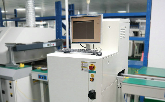
- Online AOI inspection
Inspection Purpose: To check whether there is any error, leakage or defective material flow out of the next process.
- SMT first piece inspection
Inspection purpose: To confirm the correctness of the production line mounting process and to ensure that the parameters of each resistive component are within the standard range.
- IPQC product inspection
Inspection Purpose: To randomly check all the production processes to see if they are in line with the work instructions.
- Offline AOI inspection
Inspection purpose: according to IPC610D standard inspection, the completion of the soldering of the surface mounted PCBA error leakage anti-virtual connectivity of the bad to check
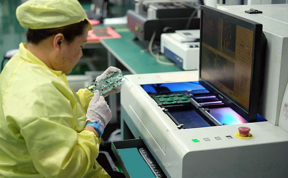
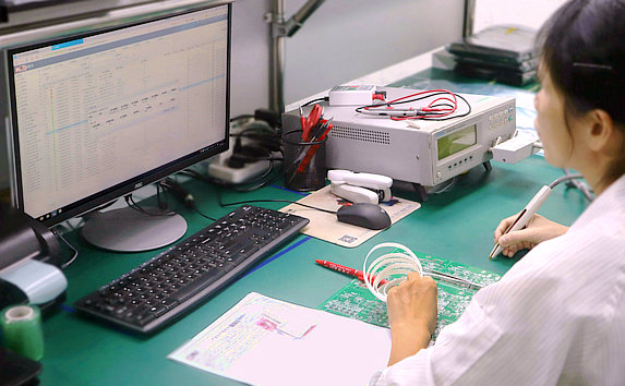
- X-RAY Inspection
Purpose of inspection: To inspect the solder joints of the original parts that are not visible to the naked eye, and to ensure the reliability of each solder ball of BGA.