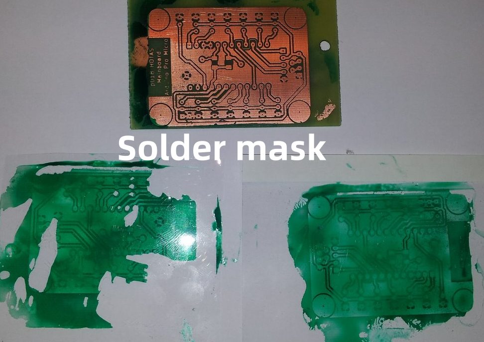
A solder mask, also known as solder resist, is a thin lacquer-like layer of polymer that is applied to the surface of printed circuit boards (PCBs) to protect the copper traces from environmental damage and prevent solder bridges from forming between closely spaced solder pads during assembly. This protective insulator coating is one of the final finishing steps performed when fabricating a PCB after etching and before board population with components.
Understanding the roles and properties of the solder mask provides key insights into PCB design strategies and manufacturing processes.
Functions of a Solder Mask
Some of the main reasons solder mask lacquer is universally applied across industrial and consumer PCBs include:
Environmental and Mechanical Protection
solder mask
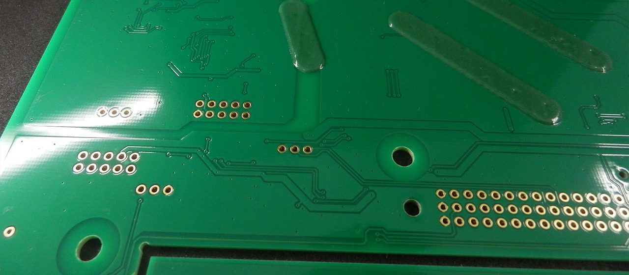
Solder mask prevents oxidation and corrosion of exposed copper conductors. It seals out moisture, contaminants, debris, etc. The coating also serves as a dielectric barrier to prevent shorting between traces in humid conditions or under electrical bias.
Additionally, the tough mask protects fragile copper traces from mechanical wear or scratches during handling and assembly. It prevents copper wicking along glass fibers in FR-4.
Preventing Solder Bridges
Probably the most vital purpose of solder mask is to act as a solder dam during component mounting. Open areas over pads define the allowable solderable regions. This prevents bridges and shorts between adjacent pins.
Insulation of Conductors
The mask delineates active circuitry from inactive areas. Bare circuits are selectively exposed while the rest of the board is insulated by the polymer which has a typical dielectric strength over 200 V/mil.
Improved Solderability
Most solder masks today feature a “solderable” epoxy formulation permitting non-conductive nickel/gold, immersion silver or organic solderability preservative (OSP) finishes to be applied over the mask for enhanced solder wetting.
Marking and Identification
Solder mask color allows easy board recognition and application identification. Different colors, textual legends and logos can be printed. Automated optical inspection depends on mask contrasts.
In summary, solder masking is a mandatory processing step for all but the most trivial PCB designs to ensure both reliability of the finished circuit and efficiency of manufacturing.
Solder Mask Types
There are two major categories of solder mask materials used in PCB fabrication:
Liquid Photoimageable Solder Masks (LPISM)
- Dominant technology – over 75% of PCBs
- Applied by screen printing, curtain coating or spray methods
- Photoinitiators allow UV light imaging
- Developed with alkaline solution to reveal solder lands
- Thermally cured epoxy-based polymers
Dry Film Solder Masks (DFSM)
- Sheet-type photopolymers laminated onto PCBs
- More consistent thickness control
- Reserved for finer pitch designs or special requirements
- Costlier than liquid masks
Within both groups, a number of solder mask material options exist with different performance trade-offs.
Liquid Solder Mask Resin Chemistries
Epoxy formulations offer very high adhesion strength to copper and FR-4 along with chemical/temperature resistance suited for most applications. They require lengthy thermal curing and have relatively poor flexibility.
Acrylic masks sacrifice some adhesion and chemical resistance versus epoxies but enable faster UV curing. They feature better flexibility and dielectric properties.
Silicone and Urethane masks provide the highest flexibility, tear strength and thermal shock resistance but have greater raw material costs. Adhesion can also be an issue.
Hybrid solder masks combine resin types to balance performance. Acrylic-epoxy allows faster curing than pure epoxy while retaining strong copper bond strength.
Typical Liquid Solder Mask Properties
| Property | Value Range |
|---|---|
| Temperature Resistance | -55°C to 150°C |
| Dielectric Constant | 3.5 – 4.5 @ 1MHz |
| Thickness | 25-75 um |
| Copper Peel Strength | > 1.3 kg/mm |
| Insulation Resistance | > 1 x 10^12 ohm-cm |
| Dielectric Breakdown Voltage | >1500 VAC |
| Coefficient of Thermal Expansion (CTE) | ~35 ppm/ |
| Flame Resistance | UL-94 VTM-0 rated |
Solder Mask Processing
Applying a reliable solder mask with accurate opened/closed patterns is a multi-stage photographic imaging and development process.
Key Steps Generally Include:
- Surface Preparation – Thorough PCB cleaning followed by optional adhesion promoter application
- Liquid Mask Print Application – Screen, curtain or spray coating to achieve 25-100 μm film
- Soft Bake – 60-100°C bake removes solvents/moisture prior to imaging
- Exposure – UV light transferred through a negative film mask hardens exposed areas
- Developing – Unpolymerized mask washed away with alkaline developer revealing lands/features
- Final Curing – Heat or UV light fully polymerizes the photoimageable mask pattern
- Post Treatment – Cool down and optional surface finish applications like ENIG, immersion silver, etc.
- Automated Optical Inspection – Verifies solder mask quality and opened contacts before assembly
Maintaining process control parameters like temperature, exposure energy, developer concentration and rinse proficiency is necessary to generate a void and pin-hole free mask with accurately defined openings.
Solder Mask Design Guidelines
To leverage the protective and functional benefits of solder masking, certain layout practices are recommended:
- Mask all unused areas of assembled boards besides exposed solder pads
- Specify 8-12 mil mask dams surrounding exposed pads
- Increase mask web width for higher density interface pads
- Apply global solder mask expansion offset (5 mil typical)
- Restrict mask openings sizes to 1.2-2X the pad size
- Select darker mask colors for better contrast than base laminate
- Include fiducials and alignment marks for manufacturing recognition
- Print reference designators, polarity indicators, board name, etc.
Advanced Solder Mask Capabilities
With 30 years of material and process innovations, today’s PCB solder masks offer capabilities far beyond simple insulation:
Controlled Thickness – Tighter control down to ±8 μm now achieves finer pad spacing without risk of bridging during assembly. This enables microvias, 0.3mm BGAs, 01005 passives, etc.
Reduced Curing Time – Fast exposure resins enable some masks to fully cure in under a minute. This supports faster PCB fabrication through-put.
Halogen-Free & Fire Resistance – Most masks no longer emit toxic fumes when burned. UL and IPC certification is standard.
Flexible and Stretchable Mask Properties – Special masks accommodate flex-rigid bending or structural electronics circuits which see physical elongation.
High Temperature Resistance – New formulations withstand over 280°C temporarily and 130-150°C continuously without issue.
Direct Metallization Capability – Nickel, gold, silver and even copper can now be directly plated onto some solder masks without separate adhesion treatments.
Improved Aesthetics – Glossy and colored masks are printable for branding graphics, text info, pin designators, and hidden metallic symbols detectable under UV blacklight.
Laser Ablation – Solder masks designed for direct structuring by laser direct imaging tools further streamline advanced PCB prototyping and ramp-up.
Common Solder Mask Defects
Despite rigorous quality controls, solder masks still risk certain failure modes affecting PCB reliability:
| Defect | Description | Cause |
|---|---|---|
| Voids | Regions with missing mask film coverage over base laminate. | Poor drill hole cleaning. Incomplete curing. Insufficient development. Poor copper surface adhesion prep. |
| Tenting | Sagging mask material partially covering drilled holes or vias. | Inadequate pre-heating. Too thick mask application. Weak developing. |
| Pinholes | Tiny mask perforations exposing base laminate. | Dust contamination. Air bubbles from mixing. Too thin film. |
| Craters | Discrete mask divots with exposed centers. | Surface contamination preventing mask wetting like oils, fluxes or oxidized copper. |
| Blistering | Small thin-walled bumps under the mask surface. | Moisture absorption into the mask film. |
| Delamination | Regions of detached mask films with poor interlayer adhesion. | Inadequate surface prep. Copper oxidation. Weak curing. Thermal shocks. |
| Solder Beading | Non-wetting solder buildup effect on SMD pads during assembly. | Mask contamination from hand oils, flux or patination preventing solder alloy wetting. |
| Bridging | Unintended solder connections between adjacent pads from excess solder. | Insufficient web width between dense pads. Poor assembly parameter control. |
Role of Solder Mask in Assembly
Since a primary function of solder mask is controlling solder paste deposition and defining non-wettable areas during component mounting, factors like minimum web width, expansion offsets and pad opening dimensions carry significance.
Insufficient openings or clearance gaps risk assembly faults:
- Solder Starvation – Too small mask apertures restrict paste transfer onto pads starving joints.
- Mask Bridges – Webs below 4-6 mils may allow solder to wet across during reflow or rework.
- Solder Balling – Excess paste squeezing out from mask-defined voids risks shorts, icicles, etc.
Conversely, excessively enlarged pad openings reduces masking protection and wastes solder paste. Finding the right balance through intentional design strategies maximizes assembly yield and reliability.
Solder Mask Finish Interactions

Across the PCB fabrication workflow, application of final surface finishes represents the last production step after solder mask with the two layers interacting:
OSP Coating – Widely used entails stabilized organic acids that react with pad copper to form a thin protective skin. Must sit on top of solder mask with no laminar voids.
Immersion Silver – Electroless deposition of silver builds up a solderable finish. Adhesion to mask varies but is normally adequate.
Immersion Tin – Similar electroless plating process but deposits tin instead. Can dissolve copper creating voids if capillary actions undermines the mask.
ENIG (Electroless Nickel Immersion Gold) – Combines nickel corrosion protection under a gold alloy outer layer. The nickel component can induce mask detachment without special secondary bonding treatments.
HASL (Hot Air Solder Leveling) – Flood coats the assembly with molten tin/lead or tin/copper solder. The thick metal transfer can crack or delaminate more rigid masks upon cooling.
In general, liquid photoimageable solder masks offer better compatibility with common finishes compared to dry film masks which require extra chemical or mechanical roughening steps to promote metal plating adhesion.
FQA
What is the main purpose of applying solder mask to PCBs?
The primary functions of solder mask are preventing solder bridges from forming between adjacent pads during assembly by acting as a dam or barrier, and protecting exposed copper conductors on the PCB surface from environmental corrosion and mechanical wear.
Does solder mask go over the entire PCB?
Nearly all PCB surface area besides the actively soldered component pads get covered by solder mask for insulation and protection. Small regions may remain unmasked for testpoints or other design needs. Board edges are typically left uncoated as well.
What methods are used to apply liquid solder mask?
Screen printing and curtain coating are the predominant application methods to deposit the 25-100 μm liquid solder mask films onto prepared PCBs before photoimaging and curing. Spray coating is also used but risks greater thickness variations.
How does photoimaging define the solder mask pattern?
Similar to photoresist patterning of copper plating, UV light passes through a negative film onto the liquid mask which locally polymerizes exposed areas. Subsequent developing washes away unexposed mask from pad locations that must remain open.
What are some key considerations when designing solder masks?
- Allow 8-12 mil mask web clearance around exposed landing pads
- Apply 5 mil global solder mask expansion offsets from copper edges
- Restrict mask openings to no larger than 2X the pad size
- Include reference fiducials and polarity indicators
- Print board name, text info, and symbols using the mask ink


