Printed circuit boards (PCBs) are designed to mechanically support and electrically connect electronic components using conductive traces etched from copper sheets laminated onto a non-conductive substrate. But PCBs also need to effectively dissipate the heat generated by components to ensure reliable operation. This is where thermal vias come in.
Thermal vias are conductive pathways formed in the PCB to transfer heat efficiently from the board to the other side or to inner ground and power planes. This heat sinking ability allows proper cooling of heat-sensitive devices.
In this comprehensive guide, we’ll explore what thermal vias are, their design considerations, how they work to cool PCBs, and best practices for their implementation. Proper use of thermal vias provides a critical thermal management solution for high power and tightly packed PCB assemblies.
What are Thermal Vias?
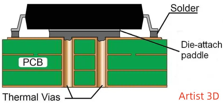
Thermal vias are plated through-holes (PTHs) in a PCB that transfer heat between the surface layers and inner plane layers of the board through metal conduction. Filling these vias with thermal epoxies or solder creates solid metal poles spanning the PCB layers.
Vias containing no traces act solely as thermal conduits to conduct heat away laterally and vertically. This gives the heat a path to dissipate across the entire board and to attached heat sinks. The vias form tunnels that channel heat from hot components, through dielectrics, spreading it over broader cooler areas.
Functions and Benefits of Thermal Vias
What key functions do thermal vias perform?
Heat Conduction
Vias provide a low thermal resistance path for heat to flow from sources to sinks or plane layers, preventing localized hot spots.
Heat Spreading
They disperse and spread concentrated heat over larger PCB volumes for more effective dissipation.
Component Cooling
Thermal vias allow mounting hot components like CPUs closer together without overheating by efficiently exporting their heat.
Plane Coupling
Vias transfer heat to inner ground and power planes which act as heat spreaders due to their large surface area.
Sink Attachment
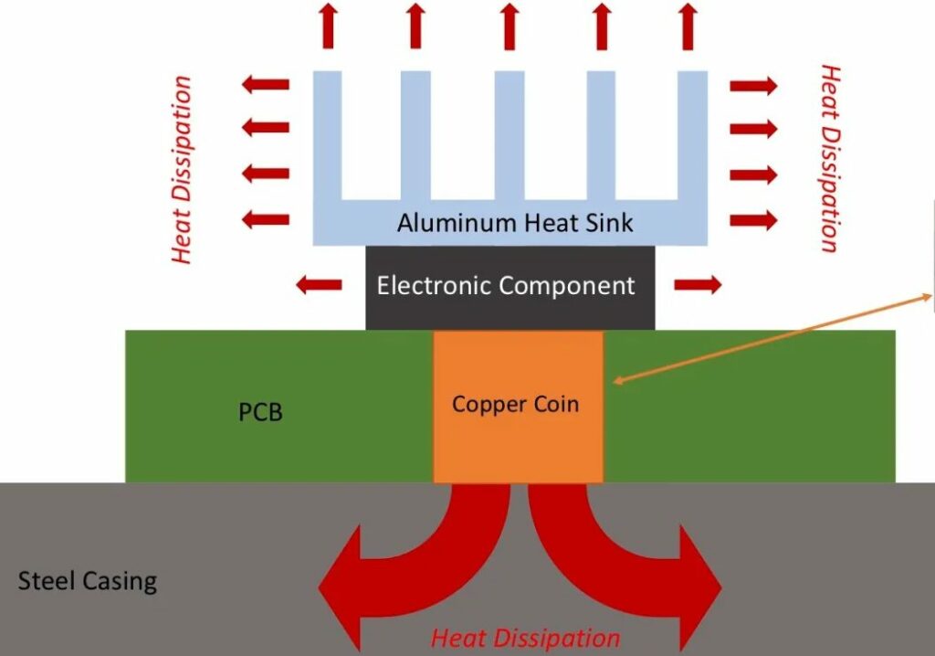
Vias facilitate conduction of heat to external cooling devices like heat sinks attached to board.
Improve Reliability
Regulating board temperature fluctuations improves circuit stability and prevents thermomechanical failures.
In summary, thermal vias enable cooling of densely packed high power electronics to ensure proper function.
Thermal Via Design Considerations
Several factors should be considered when engineering vias as part of a PCB thermal management system:
Quantity
The number of vias proportional to heat load – high power components require more vias.
Placement
Vias should be close to heat sources and evenly distributed for spreading.
Size
Wide vias have lower thermal resistance but require more space.
Depth
Vias should span entire board thickness to contact all layers.
Material
High conductivity metals like copper maximize heat transfer.
Fill Composition
Solder, epoxy, pressed metal provide lower resistance than hollow vias.
Wall Metal Plating
Thicker plating deposits minimize thermal resistance.
Anti-pad Size
Larger anti-pads lowers conduction from sources but requires more area.
Optimized via quantity, placement, dimensions and materials are essential to effectively lower PCB thermal resistance.
How Thermal Vias Work
Thermal vias function based on the physics of conductive heat transfer. Here are the key operating principles:
Metal Conduction
The metals forming vias – copper, solder, etc. have high thermal conductivity, allowing heat to readily flow through them.
Increased Contact Area
Vias provide more contact surface between layers for heat to spread into.
Reduced Dielectric Insulation
Less insulating dielectric material exists in the via path compared to PCB laminate.
Vertical Heat Pipeline
Vias form a direct vertical conduit for heat flow instead of needing to diffuse laterally across a board.
Plane Spreading
Large area ground and power planes dispersed heat out through their expanse.
Multi-Layer Coupling
Vias couple all layers together into a 3D heat conduction network.
In summary, vias provide lower resistance pathways to effectively distribute heat across PCB volumes and avoid localized hot spots.
Thermal Via Geometries
Several thermal via designs exist, allowing optimization for factors like space constraints, required heat conductance and manufacturing considerations:
Through Hole Vias
- Drilled holes spanning entire board thickness
- Maximum conduction but requires drilling
Blind & Buried Vias
- Holes stopping at inner layers
- Conserve surface area but less vertical heat transfer
Microvias
- Small diameter vias (≤ 0.15mm)
- Higher density packing but thinner metal walls
Skip Vias
- Skip alternating pad connections
- Lower density for spacing Constraints
Annular Ring Thermo-Vias
- Solid central pillar surrounded by a ring via trench
- Very low resistance but challenging fabrication
Matching via geometry to layout and performance needs results in an efficient thermal conduction network.
Thermal Via Placement Guidelines
Proper via placement is key to creating effective heat flow paths:
- Around heat generating components
- Along hot signal trace routes
- Near edges for lateral heat spreading
- Distributed across PCB area
- Under exposed pad IC packages
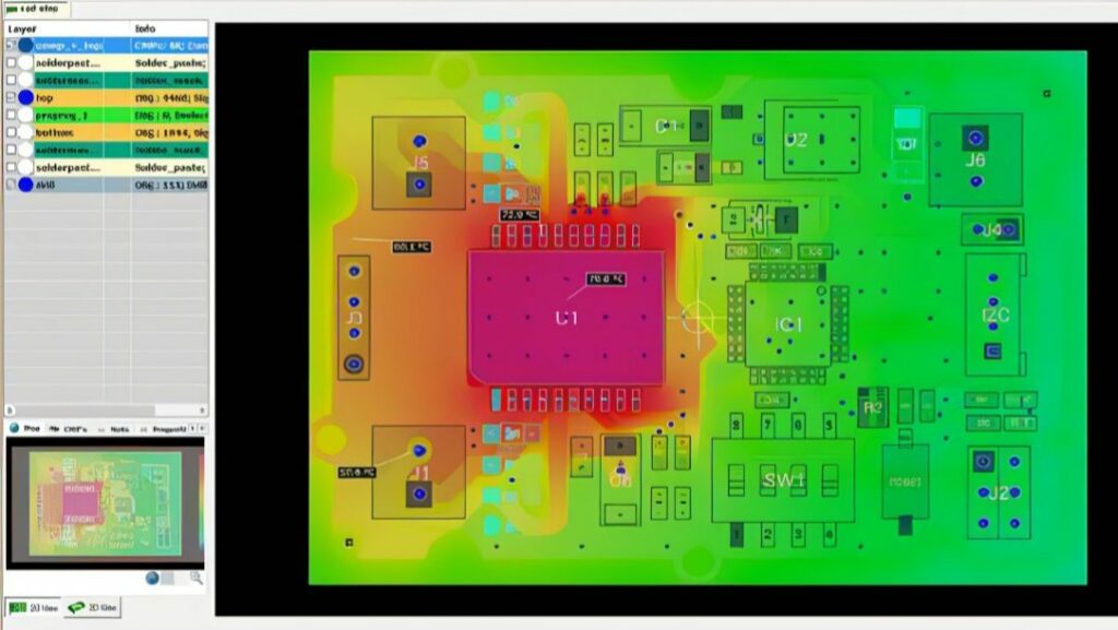
- Under hot spots seen in thermal imaging
- Along anticipated heat flow paths
- Connecting to inner layer planes
- Clustered around heat sinks
Evenly spacing vias allows heat dissipation over the maximum PCB area. Strategic localized densification focuses cooling where most needed.
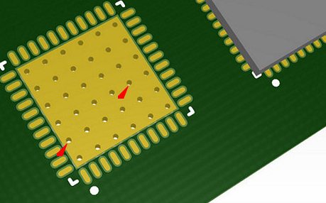
Thermal Via Pattern Examples
Common thermal via distribution patterns:
Grid Array
- Vias in regular grid across PCB surface
- Spreads heat evenly over area
Buried Grid Array
- Grid array on inner layers
- Makes space for routing on outer layers
Localized Clusters
- Dense groups of vias near hot spots
- Maximizes local heat dissipation
Radial Heat Sinks
- Vias distributed radially around heat sources
- Mimics heat spreader fins
Chassis Mounting Patterns
- Vias placed near chassis mounting holes
- Facilitates heat transfer to enclosure
The optimal pattern balances even spreading and targeted cooling.
Thermal Via Filling Materials
Filling vias improves conductance. Common via fill options:
Solder
- Highly thermally conductive
- Can be done by reflow process
- Risk of solder leaching from plating
Conductive Epoxy
- Nearly as conductive as solder
- Environmentally stable
- Higher cost
Copper Plugs
- Pressed solid copper inserts
- Matches thermal expansion to copper
- Challenging insertion process
Silver Filled Epoxy
- Excellent thermal performance
- Very expensive
- Mostly reserved for aerospace
Fill materials should be selected based on thermal needs, manufacturing constraints, and budget.
Thermal Via Filling Process
Main methods of depositing fill material:
Molten Reflow
- Pre-fluxed PTHs flooded with solder paste then reflowed
- Fast and simple process
Screen Printing
- Fill pastes/inks squeezed into vias using stencils
- Requires solder masks clear of vias
Jetting
- Precisely dispenses fill material droplets into vias
- Allows varied fill levels and patterns
Plating
- Electrolytic process builds up fill metal thickness
- Tightest void control but slower
An optimal and efficient via filling process results in low voids, strong adhesion, and minimal overfill.
Thermal Via Plating
Plating the drill walls improves conductance:
Thickness
- Total plated metal thickness should exceed 20 microns
- Thicker is lower resistance
Plating Options
- Electroless copper – moderate cost, slower
- Electrolytic copper – quicker, lower resistance
- Silver – extremely conductive but expensive
Anti-pad Plating
- Should match via plating to avoid bimetallic effect during thermal cycling
Maximizing plating thickness reduces via thermal resistance but increases fabrication costs.
Thermal Via Design Tradeoffs
Optimizing thermal vias requires balancing tradeoffs:
| Benefit | Drawback |
|---|---|
| More Vias | Consuming routing space |
| Larger Vias | Harder PCB fabrication |
| Blind/buried Vias | Less vertical heat transfer |
| Thicker Plating | Higher Manufacturing Cost |
| Solder Filled | Risk of Solder Leaching |
| Copper Filled | Challenging Insertion Process |
| Silver Filled | Very Expensive |
Careful design analysis balancing all factors results in the ideal thermal via implementation.
Thermal Via Implementation Guidelines
Follow these best practices when using thermal vias:
- Add 10-20% extra vias to account for fill voids
- Ensure complete filling to prevent traps
- Request thicker plating from fab house
- Favor many small vias over fewer large ones
- Place vias on non-critical signal layers
- Assign to automated planes rather than manual routing
- Keep anti-pads clear of other drill holes
- Avoid shaping copper pours around vias
- Request impedance modeling if vias interact with traces
- Share vias between components if possible
- Verify expected conductivity improvement through thermal modeling
Proper design, fabrication, assembly, and verification ensures thermal vias deliver their full cooling potential.
Thermal Via Design Guidelines per PCB Class
Recommended thermal via approaches by PCB class:
| PCB Class | Recommended Via Style |
|---|---|
| Class 1 | 2:1 blind/buried ratio |
| Class 2 | 1:1 blind/buried ratio |
| Class 3 | 100% through hole vias |
Matching via types to fabrication complexity minimizes costs.
Thermal Via Implementation – FQA
Here are answers to some frequently asked questions about implementing thermal vias:
Should every plated through-hole be converted to a thermal via?
Making all PTHs into thermal vias is usually overkill and unnecessary. The functions can be kept separate where appropriate. Vias that already serve an electrical interconnect purpose typically do not need to be thermally optimized. Reserve thermal vias for where maximum heat dissipation is needed.
Is there an ideal thermal via wall copper thickness?
As a rule of thumb, target plating thickness of 20 microns minimum for good thermal performance, with 25-30 microns or more being ideal. Too thin of a plating layer increases resistance. But extremely thick plating becomes prohibitively expensive and provides diminishing returns.
Do thermal vias increase EMI compared to solid ground planes?
By piercing plane layers, thermal vias can allow more EMI leakage compared to a continuous unbroken ground plane. But this effect is generally small, local, and outweighed by the substantial thermal benefit of thermal vias. Small keepouts around any sensitive areas prevents leakage.
Is it better to have a few large or many small thermal vias?
For a given via area, multiple smaller vias provide lower thermal resistance than one large via. The increased perimeter and surface area improves heat transfer. But very tiny microvias risk poor filling and plating deposition. A balance should be struck based on manufacturing capabilities.
Can thermal vias be placed in the solder mask opening areas?
It is preferable to keep vias out of solder mask openings when possible. During reflow, solder can wick down into filled vias, potentially depleting solder from pads and causing defects. An exception is skipping vias between pad connections.
Conclusion
Thermal vias provide a critical means of conducting heat efficiently within a PCB to avoid excessive component temperatures. By reducing thermal resistance, thermal vias enable proper cooling of densely packed and high power electronics. Their careful implementation during the design phase is key to creating PCBs that can operate reliably without overheating. With an understanding of the principles behind thermal via operation, designers can strategically leverage these beneficial structures. Thermal vias form a cornerstone of electronics thermal management alongside heat sinks, airflow and thermal interface materials.


