Design
-
What is Signal Propagation Delay in a PCB?
Posted by
–
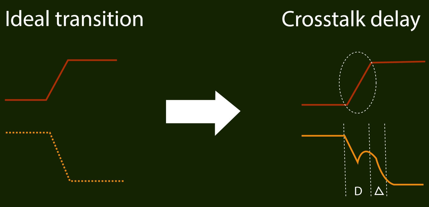
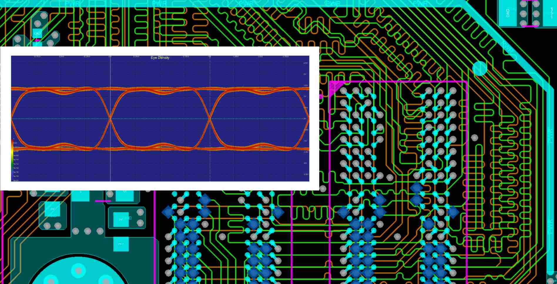
Read more: What is Signal Propagation Delay in a PCB?In high speed PCB design, signal propagation delay defines the time taken for electronic wavefronts to traverse interconnects from drivers to receivers. With data rates exceeding multi-gigabits per second, delay directly impacts timing budgets. Understanding key contributors that make up propagation delay enables engineers to model, analyze and optimize high … Read more
-
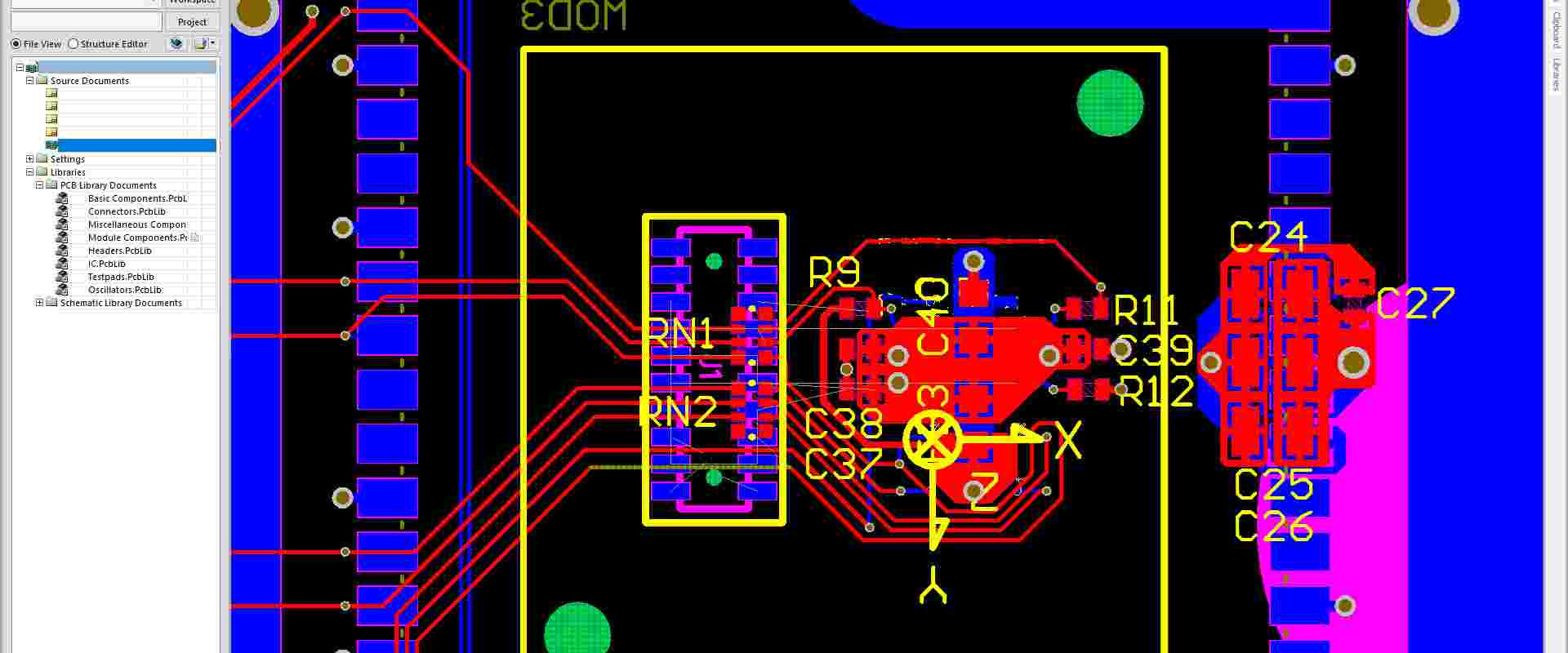
What is Protel PCB?
Posted by
–
 Read more: What is Protel PCB?
Protel PCB was one of the early and widely used printed circuit board (PCB) design software tools for electronic engineers to lay out boards. Originally created by Labcenter Electronics in the UK, Protel became popular in the 1990s for schematic capture and PCB layout. The technology and brand name got … Read more
-
20 Factors that Impact RF PCB Design
Posted by
–
 Read more: 20 Factors that Impact RF PCB Design
Designing a Printed Circuit Board (PCB) for Radio Frequency (RF) applications is vastly different from designing a board for typical digital logic applications. Even small changes in layout geometry or component selection can make the difference between a board that achieves the desired performance vs one that underperforms or is … Read more
-
 Read more: The Digital Engineer’s Guide to RF PCB Design Guidelines (2024Updated)
Radio frequency (RF) printed circuit boards (PCBs) are becoming ubiquitous across industries as wireless connectivity gets integrated into products like smartphones, vehicles, IoT devices, communication infrastructure and so on. However, RF design practices have remained a “dark art” relegated to specialized roles. This article attempts to bridge the gap by … Read more
-
 Read more: Rigid Flex PCB Design Guidelines for Manufacturing
Rigid flex PCBs rigid flex pcb design guidelines combine rigid printed circuit boards and flexible printed circuit boards into a single interconnected assembly. By incorporating both rigid sections and flexible folds, rigid flex allows conformal adaptation to space constrained 3D enclosures found in products like foldable mobile devices, wearables, medical … Read more
-
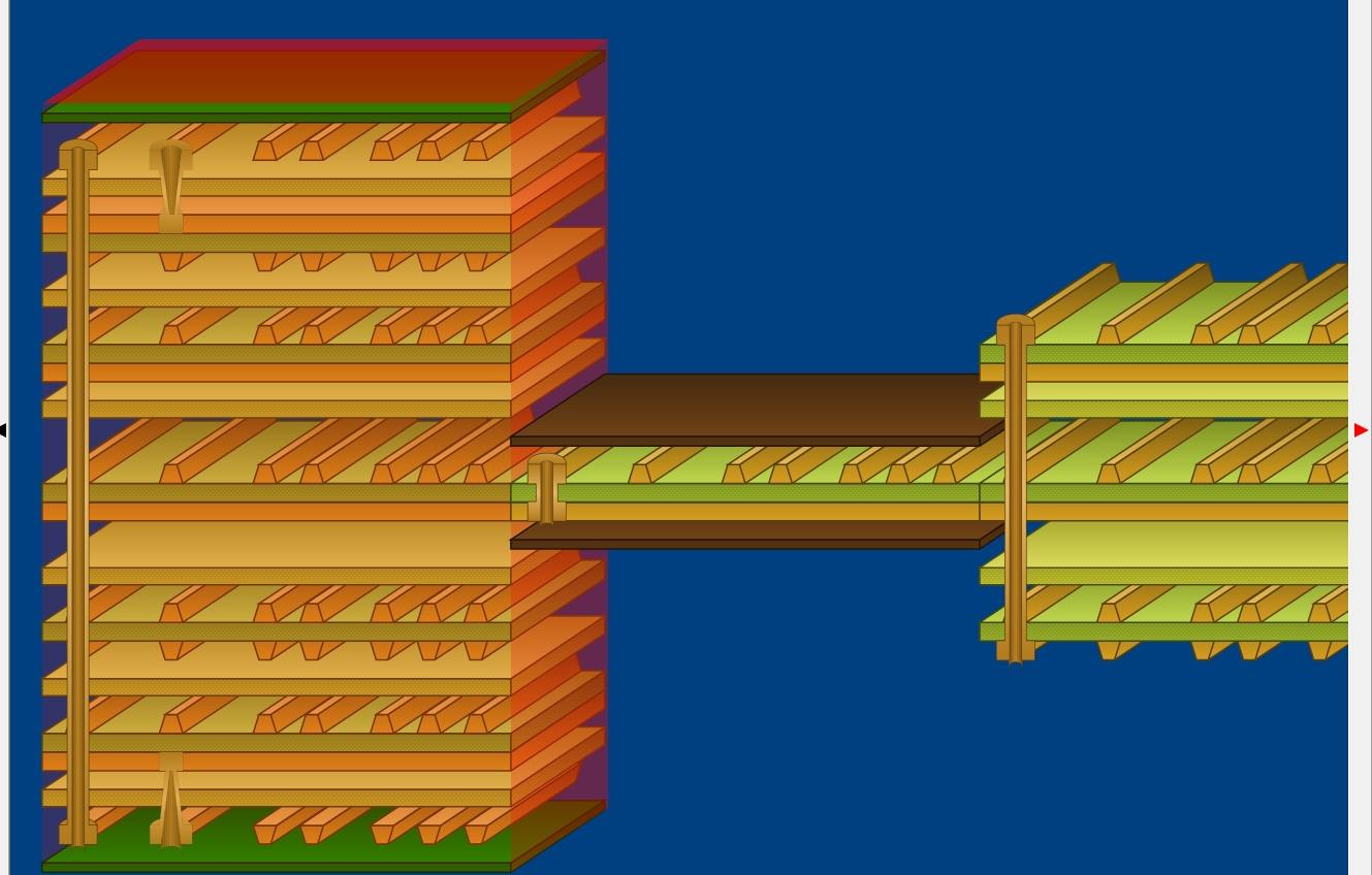
How to Design Rigid Flex PCB Stackup
Posted by
–
Read more: How to Design Rigid Flex PCB StackupA rigid flex PCB (also known as rigid flexible printed circuit board) combines rigid PCBs and flexible PCB circuits together into one interconnected PCB unit. They provide solutions when dealing with complex interconnections between components in limited spaces and for applications where flexible and dynamic motion or vibration is involved. … Read more
-
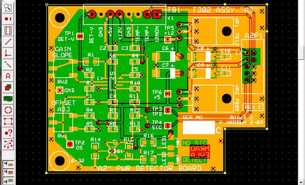 Read more: How to Convert Schematic Diagram into PCB layout?
A printed circuit board (PCB) serves as the physical platform that electronically connects components using copper traces etched from laminated sheets. The PCB Layout is designed based on the electrical connectivity described in the schematic diagram. This guide covers the following aspects involved in transforming a schematic into the corresponding … Read more
-
Looking for PCB Design Serice in Shenzhen
Posted by
–
 Read more: Looking for PCB Design Serice in Shenzhen
Shenzhen is known as the electronics and manufacturing hub of China, with a huge ecosystem of companies specializing in PCB (printed circuit board) design and manufacturing. As products continue getting more compact and complex, the PCB design process requires more sophisticated tools and expertise. This makes choosing the right PCB … Read more
-
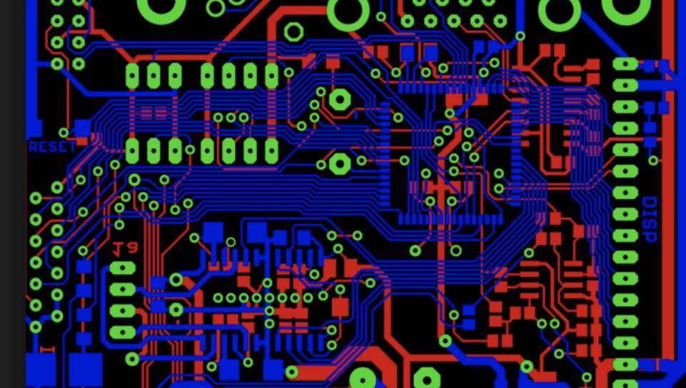
 Read more: How to Improve Signal Integrity in PCB Design (Guidelines)
As electronics become faster with data rates exceeding Gbps speeds, ensuring flawless signal transmission across PCB interconnects proves imperative for reliable functionality. However, several parasitic electrical phenomenon during high speed signaling can accumulate degrading waveform quality – falling under the discipline of signal integrity. This comprehensive guide covers common signal … Read more
-
 Read more: How to Import Footprints and Symbols from SnapEDA
SnapEDA offers a free cloud library containing over 500,000 ready-to-use CAD models for electronic components, including schematic symbols and PCB footprints. This covers common parts like resistors and caps to complex ICs, connectors across all manufacturers serving prototype to production needs. PCB and schematic footprint availability remains one of the … Read more
Recent Posts
- Understanding the PCB Burn-in Testing Process in PCB Manufacturing!

- Unlock the Potential of Embedded PCB Assemblies for Improving the Performance of Electronics Devices

- What are the Advantages of Custom Cable Assembly to meet your bespoke needs?

- What are the benefits and limitations of custom PCB boards?

- What are the benefits of Prototype PCB manufacturing and why is it important?

Categories
- 3D Guides 2,663
- Components 4
- Design 22
- Electronics 20
- PCB 125
- SMT 27
Tag Cloud
There’s no content to show here yet.