Introduction
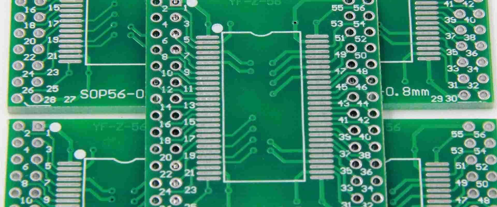
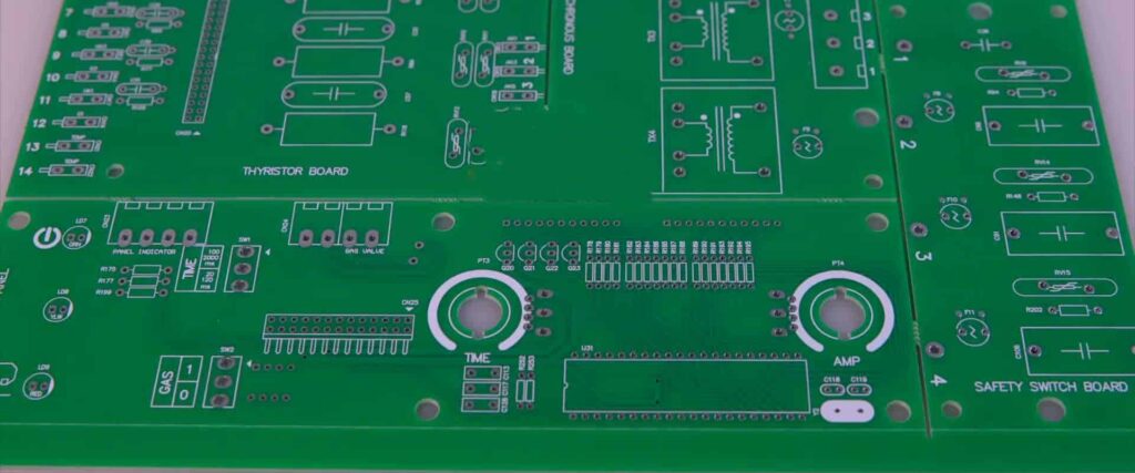
A printed circuit board (PCB) is a board used to mechanically support and electrically connect electronic components using conductive pathways or traces etched from copper sheets laminated onto a non-conductive substrate. PCBs provide the foundation for almost all modern electronic devices and equipment. They allow the fabrication of complex, compact, and reliable electronic circuits.
This article provides a comprehensive overview of PCB technology, manufacturing processes, design considerations, substrate materials, testing, and applications across different industries.
History of Printed Circuit Boards
The earliest origins of PCBs date back to the beginning of the 20th century. Here is a brief timeline showing the major developments:
- 1903 – Albert Hanson describes flat foil conductors laminated onto an insulating board in his US patent
- 1925 – Charles Ducas files a patent for a method of printing electric wiring on a board
- 1936 – Paul Eisler files a patent for a printed circuit technique while working in the UK
- 1943 – The US Army begins using PCBs in proximity fuzes for bombs to reduce wiring and assembly costs
- 1948 – The first commercial electronic device using a PCB is manufactured – the Kalabar radio receiver
- 1950s – PCBs gain widespread commercial use in industrial and consumer electronic products
- 1970s – Multilayer boards become standard as component densities increase
- 1980s – Surface mount technology drives further miniaturization of PCBs
- 1990s – High density interconnect (HDI) PCBs introduced to support complex electronics
- 2000s – Growth in flex, rigid-flex, and embedded component PCBs
PCBs have continued advancing in terms of density, performance, and capabilities to meet the needs of modern electronics. They have enabled the electronics revolution of the late 20th century.
Components of a Printed Circuit Board
A PCB consists of the following major components:
Substrate
The base material that forms the structure of the PCB. This electrically insulating material has the conductor pattern etched onto it. The substrate can be rigid or flexible.
Conductors
The copper foil traces etched onto the substrate that electrically interconnect the components mounted on the PCB. Also referred to as tracks or signal traces.
Pads
Metal areas on the substrate where component leads or interconnects are soldered. Pads connect the components to the conductive traces.
Vias
Plated through-holes that provide vertical interconnections between copper layers in multilayer PCBs. Used to route signals between layers.
Silkscreen
Printed markings that identify components, contacts, indicators and other details. Used for assembly and servicing the board.
Solder mask
Coating that protects the copper traces from oxidation and accidental contacts. Exposes only the contact pads.
Major components of a typical printed circuit board
PCB Fabrication Process
Printed circuit boards are fabricated using the following generalized sequence of steps:
- Design – The PCB layout is designed using electrical CAD software based on circuit requirements.
- Prototyping – Prototype PCBs are produced and verified before full production.
- Fabrication – Raw PCB panels are fabricated using processes like etching, drilling, and plating to achieve the board pattern.
- Assembly – Electronic components are assembled and soldered onto the fabricated PCB.
- Testing – The populated PCBs undergoes electrical testing and inspection.
- Finishing – Additional finishing steps like conformal coating. Boards are then shipped to customers.
Let’s look at some of the key PCB fabrication processes in more detail:
Etching
This process transfers the desired conductive pattern onto a laminate board. It involves:
- Coating the laminate with a photosensitive material
- Exposing the coating to UV through a mask with the circuit pattern
- Developing the coating to remove exposed or unexposed areas
- Etching away copper in unwanted regions, leaving behind the desired traces
Etching process steps to form conductive traces
Drilling
Holes are drilled through the board or between layers to create vias for component leads and interlayer connections:
- Entry and exit drill locations are aligned using fixtures
- Micro drills create the holes with high precision
- Deburring clears away drilling debris
Plating
Electrolytic plating deposits conductive copper onto the drilled hole walls to form the plated through holes (PTHs) and interconnect vias:
- Electroless plating first activates hole walls
- Electrolytic copper plating builds up conductive thickness
- Holes are electrically tested for plating defects
Lamination
Multilayer boards are fabricated by laminating together etched single layers and prepregs using high temperature and pressure:
- Layers are aligned using guide holes or optical registration
- Stackup goes through a lamination press
- Bonds layers together into a single board
Legend printing
Identifying text and symbols like component designators and polarity markings are printed on the board:
- Inkjet or screen printing transfers the legends
- UV-curable or epoxy-based inks are used
- Provides pick-and-place assembly identification
Solder mask
The solder mask coats the PCB to protect traces from environmental damage and prevent solder bridging:
- Liquid photoimageable solder mask (LPISM) is applied by curtain coating
- Mask is imaged with UV then developed
- Exposes only contact pads and features needing solder
Surface finish
A metal plating is applied to exposed copper pads and traces to enable soldering and prevent oxidation:
- Electroless Nickel Immersion Gold (ENIG)
- Immersion Silver (ImAg)
- Organic Solderability Preservative (OSP)
- Hot Air Solder Leveling (HASL)
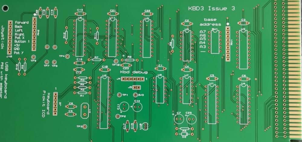
PCB Design and Layout
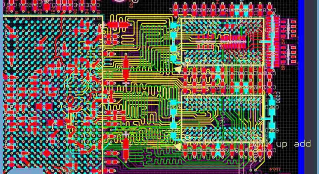
The PCB layout connects electronic components with copper traces according to circuit schematics. It is designed using specialized CAD software. Some key goals in PCB layout are:
- Placing components to minimize trace lengths
- Routing traces efficiently between connections
- Maintaining trace width/spacing to match circuit loads
- Controlling impedance for high speed signals
- Minimizing EMI/noise effects
- Providing proper power/ground distribution
- Facilitating manufacturing and assembly
Here are some key considerations in PCB layout:
Component placement
Where components are placed on the board topology. Good placement minimizes trace lengths and noise coupling. High speed components need to be close to reduce signal path lengths. Digital and analog circuits are separated to avoid interference. Grounding, power, and thermal needs guide placement.
Routing
How traces are routed between component connections according to electrical connectivity. Autorouters automate routing but often require manual trace tuning. Routing techniques balance length, layout density, timing needs, impedance, and noise reduction.
Layer stackup
Order and thickness of conductive copper and dielectric layers in multilayer PCBs. Layer count can range from 2 to over 30. Signal layers, plane layers, dielectric materials, and trace dimensions define the stackup.
Signal integrity
Applying layout best practices for clean signal transmission: impedance control, termination, vias, crosstalk reduction, controlled routing, and component placement. This is critical for high speed signals.
Electromagnetic interference (EMI)
Minimizing unwanted radiated or conducted EMI emissions from the board: small loop areas, ground planes, shielding, filtering, component placement, reduced aggressor signals, spread spectrum clocks.
Thermal design
Ensuring components operate within their temperature range and preventing hot spots on the board through techniques like thermal pads/vias, plane layers, airflow, heatsinks, and component placement.
Manufacturability
Designing the board so it can be fabricated and assembled reliably at the lowest cost. Minimizing drill counts, facilitating lamination, meeting finish requirements, allowing test points, and other production factors.
Specifications
The PCB layout adheres to electrical, mechanical, and material specifications provided in the customer product requirements document. This includes aspects like board dimensions, component locations, keepouts, tolerances, and performance requirements.
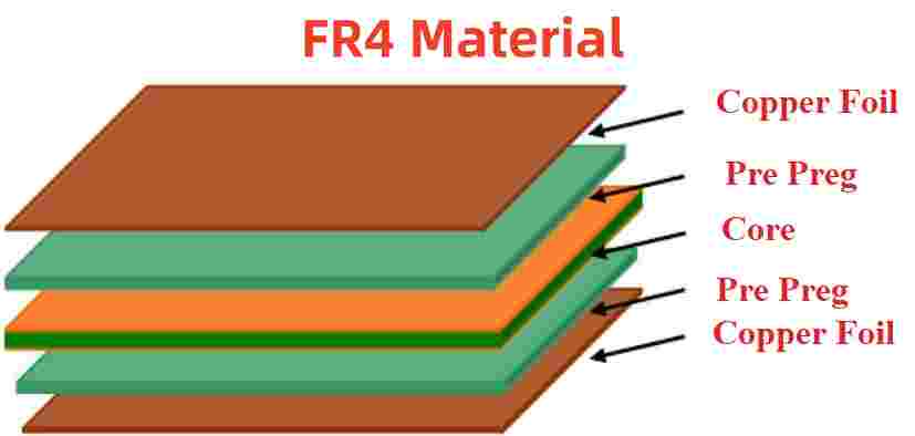
PCB Substrate Materials
PCB substrate materials provide the insulating mechanical base to which conductive layers are laminated. Here are some of the common materials used:
- FR-4 – Most common rigid PCB material. Woven fiberglass cloth impregnated with flame retardant epoxy resin. Low cost but limited high frequency performance.
- High-Tg FR-4 – Modified FR-4 with a high glass transition temperature for improved thermal and mechanical performance.
- CEM-1 – Cotton paper and epoxy composite. Low dielectric loss for high frequency applications.
- CEM-3 – Woven ceramic and epoxy composite. Very low loss and stable dielectric constant.
- PTFE – Polytetrafluoroethylene based materials like Rogers RO4000 series. Excellent high frequency characteristics.
- Polyimide – Flexible material like Kapton able to withstand bending. Used for flexible circuits.
- Isola, Nelco – High performance circuit materials from laminate suppliers like Isola, Nelco, Park, and Arlon.
The substrate choice depends on operating frequency, cost, thermal needs, flexibility requirements, and electrical performance. Advanced substrates enable higher density PCBs.
PCB Types
PCBs can be classified based on the board substrate used:
Rigid PCBs
PCBs using stiff, rigid laminate base materials that do not flex. FR-4 glass epoxy is the most common. Used in nearly all electronics from consumer devices to industrial equipment.
Flexible PCBs
Flexible PCBs use a polymer base like polyimide that can bend and flex. Used where connections need to fold or adapt to movements like in portable electronics and medical devices.
Rigid-flex PCBs
Combines both rigid and flexible substrates. Rigid sections provide mechanical stability while interconnected flex sections enable bending and flexing motion. Found in products like mobile phones.
Metal core PCBs
Use thermally conductive metal core as a central substrate layer to spread and dissipate heat. Used in LED lighting, automotive electronics, power devices.
PCB Layout Styles
Based on the routing approach, PCB layout can be classified into:
Single-sided
Conductive traces only on one side of the substrate. Least complex option but limited connectivity. Used in simple, low component count circuits.
Double-sided
Conductors on both top and bottom sides. Through-hole component leads provide interconnection between layers. Low cost but higher complexity than single-sided.
Multilayer
Has three or more conductive layers separated by insulating dielectric layers. Layers interconnected by plated through vias. Used for complex, dense designs due to routing flexibility. Most modern PCBs are multilayer.
High density interconnect (HDI)
A specialized multilayer PCB with finer trace/space dimensions, thinner dielectrics, microvias, and often blind/buried vias. Enables greater component density and miniaturization. Used in advanced electronics.
Any layer
A hybrid approach allowing traces to route on any layer without restriction. Maximizes routing flexibility. Complex to design and manufacture.
PCB Design Software
PCB layout and routing is performed using electronic design automation (EDA) software tools. Some popular options:
- Altium Designer – High-end PCB design platform with unified schematic/PCB environment.
- Cadence Allegro – Widely used suite for PCB design with engineering analysis features.
- Mentor Xpedition – Leading enterprise PCB design solution supporting team workflows.
- Eagle – Popular low-cost PCB tool, now offered by Autodesk.
- KiCad – Open-source, freely available PCB and schematic CAD application.
- OrCAD – Full PCB design solution from Cadence with high speed and signal integrity analysis.
Advanced tools incorporate signal and power integrity analysis, thermal modeling, design for manufacturing checks, version control, and team collaboration capabilities.
PCB Manufacturers
There is a large global industry of companies that fabricate printed circuit boards. Some major PCB manufacturers include:
- TTM Technologies
- Sanmina Corporation
- AT&S
- Compeq
- Chin Poon Industrial
- Tripod Technology
- Ibiden
- Unimicron Technology Corp
- Würth Elektronik Group
- Tata Chemicals ECD
In additional to large vendors, there are thousands of small local PCB fabricators worldwide. Many PCB suppliers also offer assembly services.
Testing PCBs
Printed circuit boards undergo the following testing during manufacturing:
In-circuit Test (ICT)
- Tests components and circuits electrically while still on the assembled PCB
- Precision “bed of nails” test probes contact test points and nodes
- Confirms proper assembly, verifies component values, and detects defects
Flying Probe Test
- Uses freely positioned movable test probes
- No fixtures required, adapts to different board designs
- Checks for shorts, opens, component values, etc.
Automated Optical Inspection (AOI)
- Optically scans assembled PCBs for defects and quality
- Checks component placement, solder joints, polarity, markings, etc.
- Can be 2D inspection or more advanced 3D AOI
X-Ray Inspection
- X-ray imaging used to inspect component placement and solder joints
- Primarily used to inspect and verify BGA connections
- Detects hidden or internal defects
Board Functional Test
- Stimulates inputs and monitors outputs to verify board functions correctly
- Confirms assembled board works properly before system integration
- Uses test fixture or in-circuit techniques
PCB Usage Across Industries
Printed circuit boards are ubiquitous across industrial, commercial, and consumer electronic devices. Some major application areas include:
Consumer Electronics
Mobile phones, tablets, computers, appliances, IoT devices, wearables, gaming systems, and more all extensively use PCBs to interconnect components. High volume production with stringent size, weight, and cost constraints.
Automotive
Modern vehicles contain multiple PCBs to control engine functions, sensors, infotainment, safety systems, lighting, battery management, and other automotive subsystems. Ruggedness, safety compliance, and operating temperature range are key requirements.
Aerospace and Defense
PCBs used in guidance systems, flight controls, communications, navigation, electronic warfare systems, and avionics. Reliability under harsh temperature, pressure, vibration, and radiation is critical.
Industrial
Industrial equipment uses PCBs for automation and control systems, motor drives, power supplies, instrumentation, switches, safety systems, and sensors. Environment survivability and long product lifetimes are important.
Telecommunications
Switches, routers, base stations, networking gear, and other telecom infrastructure relies on PCB technology. High frequency, noise reduction, and signal integrity requirements.
Medical
PCBs enable modern medical diagnostic systems, imaging equipment, surgical tools, implants, and patient monitoring systems by supporting complex electronics. High reliability is imperative along with regulatory compliance.
The Future of PCBs
Advances and innovations in PCB technology will enable continuing growth in electronic systems:
- Higher component density through smaller features, advanced materials, and sequential laminations
- Embedded actives with active components like ICs encapsulated within the PCB
- High speed materials like improved glass weaves and ceramic-filled composites
- Flexible and rigid-flex solutions allowing more compact three-dimensional layouts
- Additive processing like inkjet printing to complement or replace etching
- Embedded passives with thin film resistors/capacitors integrated into the PCB
- 5G communications driving materials with ultra-low loss, thermal stability, and consistency
- Automation and Industry 4.0 to improve manufacturing productivity and quality
- Advanced testing and inspection such as laminate process control, automated optical inspection, and new reliability tests
FQA
What are some key functions of a printed circuit board?
Some key functions of a PCB include:
- Mechanically supports and secures electronic components
- Interconnects components with conductive copper traces
- Distributes power and signals between components
- Facilitates component assembly through pads and markings
- Manages heat dissipation using thermal design features
- Provides physical organization and modularity to a circuit
- Electrically isolates different circuit sections
What are some differences between single-sided, double-sided, and multilayer PCBs?
Single-sided PCBs have traces on one side only. Double-sided adds traces on a second side. Multilayer PCBs have three or more conductor layers separated by insulators and interconnected by plated through holes. Multilayer provides the highest component density and routing flexibility.
What are some considerations when selecting a PCB substrate material?
Key considerations for selecting PCB substrate materials include:
- Frequency of signals the board must carry
- Required dielectric properties like loss tangent
- Thermal conductivity needed
- Cost, availability, and ease of manufacture
- Mechanical characteristics such as flexibility
- Flame retardance rating
What are some common quality tests performed on PCBs during manufacturing?
Common quality tests performed on PCBs include:
- Visual inspection of conductor pattern, spacing, and solder mask
- Testing for electrical shorts and opens
- Verifying conductive layer registrations
- Measuring dielectric layer thickness
- Testing plated through holes for continuity
- Solderability testing on surface finish
What technological innovations are influencing the advancement of PCBs?
Some innovations advancing PCB technology are: higher conductivity and lower loss materials, smaller trace/space capabilities, embedded actives and passives, additive processing methods, sequential lamination techniques, thinner dielectrics, advanced testing methods, flexible and rigid-flex materials,


