Introduction
Printed circuit board (PCB) layout is the art of arranging components and routing connections on a PCB to implement an electronic circuit. While there is significant complexity and specialization in PCB layout, adhering to some fundamental rules and guidelines will help ensure a successful board layout.
This article will provide an overview of the basic rules every PCB layout designer should follow, covering topics such as:
- Following schematic conventions
- Placement best practices
- Routing techniques
- Maintaining clarity
- Respecting manufacturing requirements
- Executing appropriate simulations
- Performing design rule checks
By internalizing these essential layout principles, PCB designers can develop robust and optimized boards.
Follow the Schematic Conventions
The first rule of PCB layout is respecting the conventions established in the schematic. The schematic and PCB should match as closely as possible in regard to:
- Circuit partitioning into functional blocks
- Hierarchical structure
- Component designators and names
- Logical grouping of related components
- Net and signal names
- Power rail conventions
- Circuit interfaces and ports
Adhering to the schematic conventions makes the layout more organized and understandable. It also simplifies schematic-to-layout cross probing and speeds up design review.
Use schematic-driven layout tools to inherit these conventions whenever possible. But be aware of any needed optimizations or deviations in laying out the board.
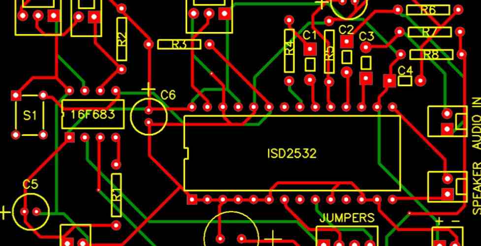
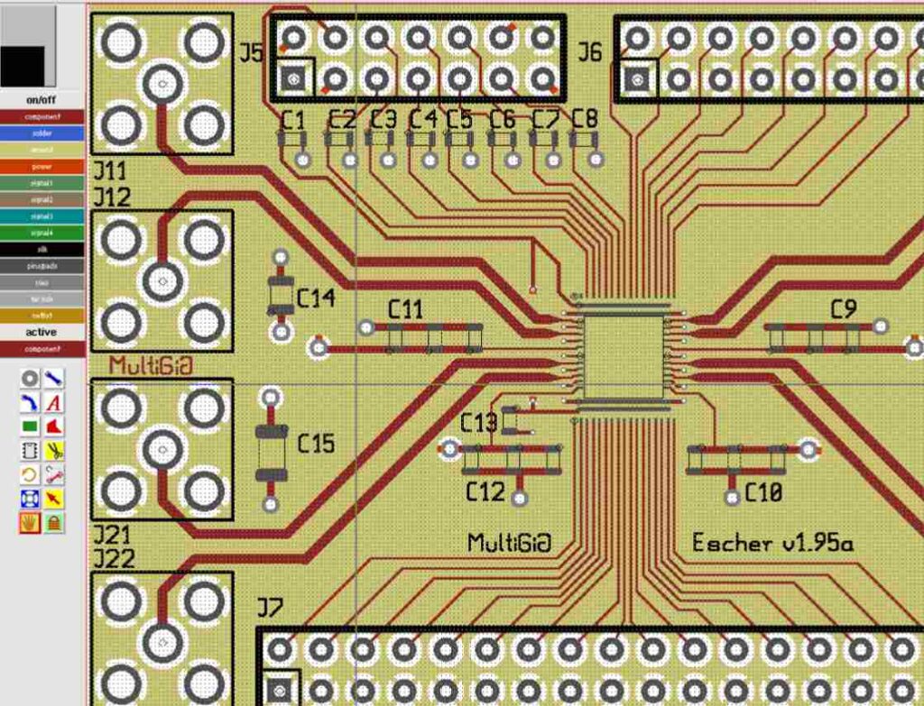
Optimize Component Placement
Component placement is a foundational PCB layout task. Good placement facilitates routing, minimizes noise, and optimizes board area utilization. Some key placement principles:
Functional Blocks
Group related components just as done in the schematic. This aids identification and serviceability. Keep associated passive components close to their active ICs.
Signal Flow
Arrange components along the path of signal flow when feasible. This reduces the length of wire connections.
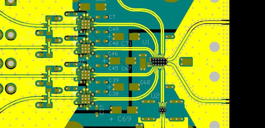
Power Components
Strategically place decoupling capacitors, voltage regulators, and power filters close to their consuming ICs. This minimizes parasitic noise in the power distribution network.
High Speed Circuits
Ensure short direct routes between driver ICs and receiver components. Minimize stubs. Careful placement is key for controlled impedance routing.
Thermals
Place heat generating components where they can be properly cooled, such as near the edge or corners of the PCB. Leave clearance for airflow or heatsinking structures if needed.
Board Constraints
Account for board dimensions, mounting holes, connectors, and any other fixed mechanical features when placing parts. Verify spacing allows assembly access.
Getting placement right is foundational for achieving routing, thermal, and signal integrity goals. Use EDA tools for initial placement but fine tune manually.
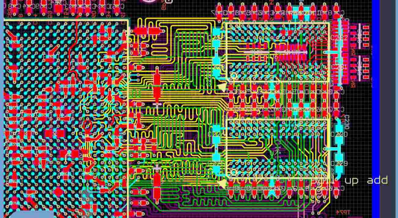
Implement Organized Routing
Routing establishes the connectivity between components on a PCB layout. Some key routing principles:
Follow Grids and Constraints
Use routing grids matched to the capabilities of your board house. Observe spacing rules defined in the design rules checklist.
Route by Net
Route all connections of a net together before moving to the next net. This yields cleaner and more organized routing.
Maintain Ideal Angles
Use primarily horizontal and vertical traces. Avoid arbitrary angled traces when possible for manufacturing and serviceability.
No Sharp Corners
For high speed signals, use curved/arc traces instead of 90 degree corners to reduce impedance discontinuities.
Minimize Crossings
Route to minimize trace crossings when possible. Use vias to cross over instead of passing two traces in intersection.
Explicit Power Connections
Clearly connect all power pins directly to their intended rails/planes to eliminate guesswork. Don’t rely on proximity.
Balance Length and Spacing
Try to match route lengths and environments for differential pairs and critical signals to control impedance. Provide adequate isolation for sensitive or noisy traces.
Inspect Serviceability
Check that routing enables access to inspect points, debugging headers, adjustable components, and connectors during assembly and servicing.
Lean routing takes time to master but following these guidelines will help build clean, readable, and manufacturable boards.
Maintain Clarity
The PCB layout should clearly convey connectivity and functionality through:
Visual Hierarchy
Emphasize important power routes and high speed signals with wider traces and differential pair spacing. Use visual cues like colors, Hugging, necking, etc.
Component Orientation
Align components properly and consistently. Use easily identified footprints. Orient text along readable axes.
Labeling and Markings
Use consistent text sizes, fonts, and colors for labels. Provide descriptive names for functional groups. Include board info like title, rev, and date.
Fill Shapes
Utilize copper fills and shapes to clearly identify large circuit nodes and planes instead of relying solely on connectivity.
Layer Stack Conventions
Adhere to recommended layer usage guidelines typical for your process and density needs.
Manufacturing Markings
Include any needed assembly or fabrication markings like thou marks, breakaway sections, grain directions etc.
While often overlooked, clarity aids manufacturability, serviceability, and review of the PCB layout.
Respect Manufacturing Requirements
PCB layouts must account for real-world manufacturing constraints:
Tolerancing
Account for typical fabrication tolerances like trace widths, hole sizes, registration, etc. in your design rules.
Spacing and Clearances
Maintain minimum spacings between traces, pads, planes, board edges. Check mask expansion tolerances.
Thermal Relief
Use thermal reliefs/spokes when routing between pad pairs to avoid pooling solder between adjacent pads.
Via Styles
Select via types suitable for your process capabilities – through hole, buried, blind, filled, plated. Minimize unsupported holes.
Impedance Control Materials
Specify materials needed for controlled impedance routing like high resin content prepregs and thickness.
Panel Utilization
Understand the board house’s panel sizes and utilization requirements to optimize fabrication yield and cost.
Test Points
Include sufficient access to test points needed for in-circuit structural testing during manufacturing.
Working within your vendors’ capabilities ensures the design is optimized for fabrication and assembly. Verify the most up to date constraints.
Perform Appropriate Simulations
Run simulations during the layout process to validate the design:
Signal Integrity
Verify signals have acceptable rise/fall times, overshoot, and impedance profiles. Identify any reflections or resonances.
Power Integrity
Check steady state supply voltages and transients remain within tolerance for all power rails under different usage scenarios.
EMI/EMC
Model radiated and conducted emissions to identify any problems meeting target emissions profiles or passing compliance requirements.
Thermal
Simulate temperatures during operation and peak conditions to ensure components are within their temperature limits given the board and enclosure design.
While simulations take time, they identify issues early when they can be addressed simply. Simulate adequately but pragmatically based on design complexity and risk areas.
Execute Design Rule Checks
Run design rule checks or DRCs to verify the physical layout meets constraints:
Spacing and Clearance DRCs
Checks for any spacing or clearance violations between traces, pads, copper, board extents, etc.
Unconnected Nodes DRC
Identifies nets with missing or unconnected nodes in the layout vs the schematic.
Unplaced Components DRC
Checks for any components missing from the layout.
Manufacturing DRC
Verifies manufacturability by checking parameters like minimum trace width, hole size, etc.
Electrical DRC
Checks electrical constraints are met like maximum capacitance, impedance tolerances, coupled noise, etc.
Performing comprehensive design rule checks is essential to confirming the layout adheres to the desired rules and constraints. Automated DRCs find potential issues quickly and reliably.
Conclusion
Adhering to basic principles of organized, clear PCB layout while respecting the schematic, considering practical manufacturing limits, simulating judiciously, and running thorough design rule checks will help ensure a successful board layout.
Layout mastery grows with experience across many designs. But following fundamental best practices from the start positions PCB designers for creating functional, robust printed circuit board layouts.
Frequently Asked Questions
What is the first key rule for starting a PCB layout?
Follow the schematic conventions for partitioning, structure, naming, power rails, and interfaces when translating to the layout.
What techniques help optimize component placement?
Group functional blocks, arrange by signal flow, place decoupling caps carefully, allow thermal clearance, and account for board space constraints.
What makes routing organized and lean?
Route signals net-by-net, use grids and constraints, avoid arbitrary angles, minimize crossings, balance lengths, and check service clearances.
How can PCB layouts be made more clear?
Use visual hierarchy, consistent component styles, thorough labeling, copper fills to identify planes, and standard layer usage.
Why is it important to consider manufacturing requirements?
To ensure the layout tolerances, spacings, and fab-specific design aspects needed to produce a functional board are respected.
When should simulations be executed during layout?
At key milestones to validate signal and power integrity, EMI/EMC, and thermal performance. Pragmatic simulation saves time and cost.
What do design rule checks like DRCs accomplish?
Automated design rule checks validate adherence to the minimum spacing, clearance, connection, and electrical constraints for proper functioning.


