
Introduction
Plated half-holes, also known as castellated holes or notched holes, are specialized holes found in printed circuit boards (PCBs) that have been “plated-through.” This means the hole has an electroplated barrel, allowing electrical connectivity between the layers of the board.
Plated half-holes are created by making small, closely spaced half-circle tabs around the perimeter of a through-hole. The spaces in between the tabs are then plated-through, forming barrel connections. This allows the hole to electrically connect multiple layers of a PCB while still allowing a component lead to pass through partway.
Plated half-holes provide several benefits, which has made them commonplace in modern PCB manufacturing:
- Allows for high-density component placement near board edges
- Facilitates right-angle soldering of leaded components
- Can act as “castellation” along board edges for modular designs
- Improves manufacturability and solderability of boards
In this article, we will explore plated half-holes in more detail, including their:
- Construction and geometry
- PCB design considerations
- Manufacturing and plating processes
- Main applications and use cases
- Advantages and limitations
- Comparisons to related hole types
We’ll also look at some examples of how plated half-holes are used on real-world circuit boards. Let’s start by understanding the structure and dimensions of these unique PCB features.
Plated Half-Hole Construction and Geometry

Plated half-holes begin life as a standard through-hole – a round opening drilled fully through a circuit board from top to bottom. During manufacturing, the hole perimeter is modified to create half-circle tabs or “castellations” around the edge.
Typical geometry of a plated half-hole
The number, size, and spacing of these tabs can vary, but typical configurations use between 8-24 tabs evenly distributed around the hole. Common tab widths are in the range of 0.2 to 1 mm. The spaces between the tabs are increased during drilling to remove the laminate material and expose the inner-layer copper.
This selectively exposes areas of the hole for plating while keeping other regions covered by the tab. During electrolytic plating of the PCB, metal builds up in the open areas between tabs, creating a conductive barrel that connects between layers. The barrel depth is usually equal to the overall board thickness but may be less.
Meanwhile, the tabs prevent plating in those areas, allowing a leaded component to pass through partway into the hole. Different tab lengths alter how deep a component lead can extend. The total diameter of the de-castellated hole is equivalent to the lead diameter of the component being mounted.
PCB Design Considerations for Plated Half-Holes
Several factors must be considered when incorporating plated half-holes into a printed circuit board design:
Component Lead Diameter
The tab length and resulting hole depth must match the diameter of the component lead that will be inserted. Thicker leads require longer tab lengths and deeper unplated regions. The lead diameter also sets the final de-castellated hole size.
Hole and Pad Size
Allowance must be made for the extra hole size needed to accommodate thetabs. For instance, to create a half-hole for an 0.8 mm component lead, the drilled hole and pad may need to be 1.2 mm or larger.
Pad Style
The pad can be an annular ring or have “thermals” (spokes) to facilitate solder flow to the plated tabs. Thermal relief pads improve solderability and reduce thermal stress on the plated joints.
Hole and Tab Spacing
The number and spacing of tabs affects the plated connection strength. More tabs provide more barrel joints but reduce the tab length. Optimal values depend on factors like current load, hole size, and plating thickness.
Tab Pattern and Orientation
Some common tab patterns are symmetrical (equally spaced), asymmetric, or clustered to one side. The orientation matters for off-angle lead insertion.
Plating Thickness
The plate thickness must be sufficient to handle the design current through the hole barrel with acceptable conductivity. Thinner plating requires more tabs and thermal relief on pads.
Routing Clearances
No traces or planes should cover the tabs or encroach on the spacing between tabs around the hole. This ensures openings exist for drilling and plating.
With these considerations in mind, let’s look at how plated half-holes are manufactured.
Manufacturing Plated Half-Holes
Fabricating plated half-holes involves several additional steps compared to standard plated-through holes:
1. Drilling
A standard through-hole is drilled in the PCB, with a bit size matching the designed full hole diameter (lead size + tabs).
High precision is required to control the hole position and size across all layers. The drilling process may elongate the hole slightly due to smearing.
2. De-casting
In this critical step, the pre-plated hole perimeter is milled, routed, or punched to create the half-hole tabs.
Modern de-casting uses mechanical milling or punching for accuracy and speed. The process must be carefully controlled to produce uniform tabs around the hole. Any asymmetry can affect soldering results.
3. Desmear
The exposed base material in the spaces between tabs is chemically cleaned using desmear solutions. This removes resin smear and debris for good plating adhesion.
4. Plating
Electrolytic copper plating builds up metal thickness on the innerlayers and on the de-castellated hole barrels between tabs. Typical plating thickness is 25 to 40 microns. The tabs prevent plating in those areas.
5. Solder masking
Liquid photoimageable solder mask (LPI) coats the board surface but avoids the tab areas and spaces between tabs. This prevents solder bridging while allowing solder fillets to form between the pad and plated barrel during assembly.
The result is a plated half-hole ready for installing leaded components. Now let’s look at some of the most common applications which take advantage of plated half-holes.
Main Applications and Use Cases
Plated half-holes are typically utilized in the following situations:
Edge-Mounted Components
Plated half-holes allow leaded components like resistors, capacitors, fuses, and inductors to be mounted along the edge of a PCB:
Example of edge-mounted radial leaded components soldered into plated half-holes
The tabs prevent the leads from passing fully through the board while the plated barrel electrically connects all layers. Right-angle lead forming allows high component density.
Castellation Plated Holes
Modules and other removable PCB sections often use plated edge holes to create a castellated interconnect:
Castellated plated half-holes connecting stacked PCB modules
When joined to another board or module, the exposed barrels form reliable solder joints. The tabs provide mechanical stability when separating the boards.
Mixed Pin Components
Some components have leads or pins of varying lengths, which can be accommodated by plated half-holes with different tab depths.
Right-Angle Sockets
Plated half-holes allow right-angle sockets and connectors to be soldered along board edges and still connect multiple layers.
Test Points
For easy probing of internal signals, plated half-holes make ideal test points when left unpopulated. The plated barrels bring signals to the edge of the board.
For these use cases, plated half-holes provide several advantages compared to regular plated-through holes.
Advantages of Plated Half-Holes
Here are some of the main benefits of specifying plated half-holes instead of standard through-hole connections:
- Higher Density: Half-holes allow components to be placed closer together and closer to board edges due to right-angle lead forming.
- Layer Interconnect: The plated barrels electrically connect between layers for components terminated at inner layers.
- No Stubbing Required: Leads do not need manual cutting or stubbing before assembly since the tabs automatically stop lead insertion.
- Stronger Solder Joints: The thermal relief shape improves solder fillet formation. More tabs provide redundancy if a joint is faulty.
- Castellation Connections: Plated half-hole edges can mate directly with other PCBs or modules.
- Mixed Lead Accommodation: Different tab depths allow components with varying lead lengths to be mounted together.
- Easier Probing: Half-holes at edges allow inner layer signals to be accessed for debugging and testing.
While very useful, plated half-holes also have some limitations and disadvantages to consider.
Limitations and Disadvantages
The main downsides of plated half-holes include:
- More Complex Manufacturing: Additional fabrication steps are required such as hole de-casting. This increases cycle time and cost.
- Larger Holes Required: The tabs increase the drilled hole size and pad dimensions. This wastes some board area.
- Limitations for Miniaturization: The tabs consume space that could otherwise be used to route traces or place components. Newer microvias provide higher interconnect density.
- Plating Voids: Poor drilling alignment or de-casting can create voids along the plated barrels, increasing resistance or disconnecting layers.
- Solder Bridging: Due to close lead spacing, bridged joints are possible requiring inspection. Solder masks mitigate this risk.
- Only for Leaded Components: Plated half-holes do not support modern surface mount pads. SMT pads require smaller microvias instead.
For applications requiring leaded through-hole components, plated half-holes are very effective. But other options exist like molded vias and microvias when maximum interconnect density is needed.
Comparison to Related Hole Types
It’s helpful to contrast plated half-holes against some other related types of plated-through holes:
- Standard Plated-Through Hole: Goes fully through the board layers. Requires manual lead stubbing or clinching. Not suitable for edge-mounting.
- Molded Via: Laser-drilled hole with resin filling. Allows stubs, buried, blind, and stacked stub connections. Higher density than plated half-holes.
- Microvia: Small laser-drilled and plated holes, usually for surface mount pads. Much higher density than plated half-holes but only for SMT parts.
- Buried and Blind Vias: Connects between inner layers but do not exit surface layers. Allow high-density routing but no component terminations.
For applications using leaded components, plated half-holes offer a unique capability beyond these other via structures. The half-plated barrels provide solderable connections while the tabs provide mechanical stability.
Real-World Applications
Plated half-holes and castellated holes appear on many types of circuit boards where right-angle leaded components are used. Some examples include:
Power Supplies
Switch mode power supplies frequently use plated half-holes along the edges to mount input/output capacitors and filter inductors:
AC-DC power supply PCB using plated half-holes for filter capacitors
The vertical capacitors help minimize loop areas for reduced EMI. Right-angle capacitor leads allow very close spacing.
LED Lighting Drivers
Similar to power supplies, LED driver PCBs often utilize plated half-holes for edge-mounted components:
![LED Driver Plated Half-Holes]1924908/Typical-LED-driver-PCB-layout-showing-plated-half-holes-and-castellated-edge-connections_Q640.jpg)
LED driver with plated half-holes around perimeter
Some times cut-outs and castellated edges are combined for compact modular boards.
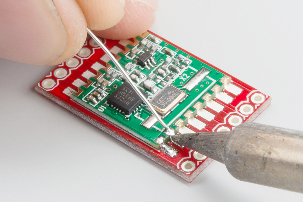
High Frequency RF Circuits
For radio frequency PCBs, right-angle connections are useful to control lead inductance. Sensitive nodes can be isolated with grounded plated half-hole shields:
![RF Circuit Plated Half-Holes]encounter individual achievement and failures by viewing those events as stepping stones to progress. Constant reflection and course-correction leads eventually to meaningful growth.”


