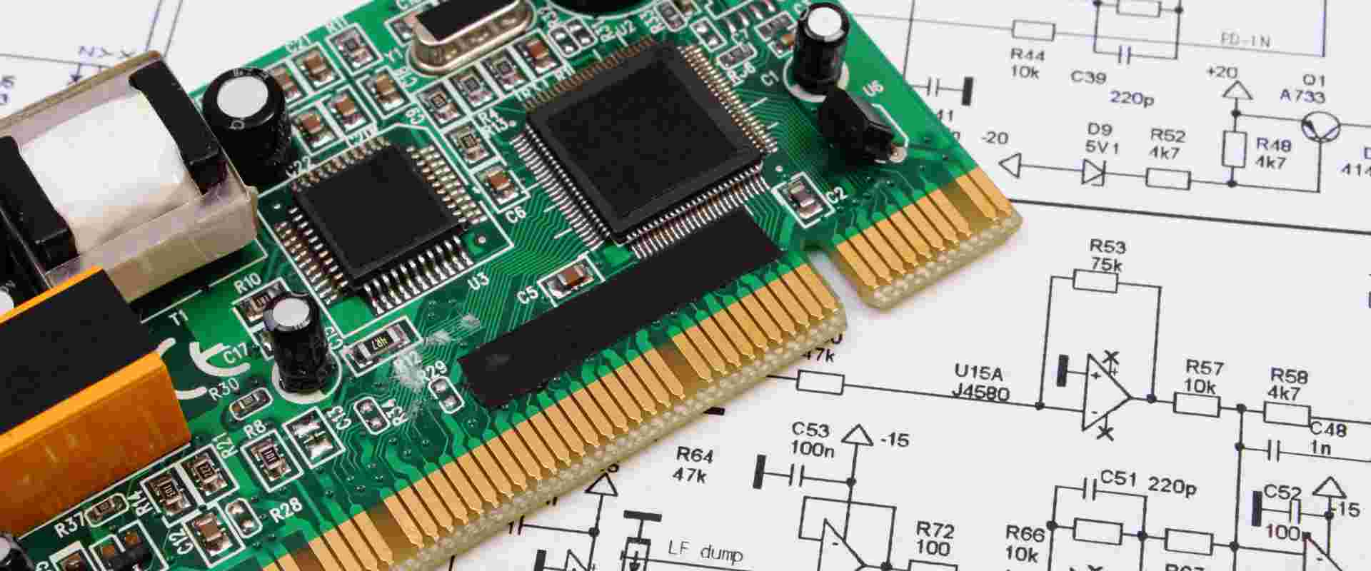
Printed circuit board (PCB) design is an essential engineering skill that allows creating the interconnect foundations of electronic devices. For innovators looking to turn concepts into functioning prototypes and products, learning PCB design unlocks tremendous capabilities. The combination of affordable consumer electronics and widely available design software has opened PCB design to makers and entrepreneurs.
Getting started in PCB design does not require an engineering degree, but it does involve learning foundational electronics principles, CAD software skills, and understanding manufacturing processes. With commitment and practice, beginners can start designing basic PCBs, then work up to more advanced boards. Here is an overview of key steps to start PCB designing as a novice.
Learn Fundamental Electronics
Electronics theory establishes critical context for PCB design work. Core concepts to grasp include:
- Circuit Fundamentals – Current, voltage, power, signals, analog vs. digital
- Resistors, Capacitors, Inductors – Passive components and their functions
- Semiconductors – Diodes, transistors, integrated circuits (ICs)
- PCB Basics – Traces, vias, layers, substrates, soldering
- Logic Gates – Boolean logic, combinational and sequential logic
- Microcontrollers – Embedded processors, input/output control
- Communications – Serial, SPI, I2C, Ethernet, wireless protocols
- Breadboarding – Prototyping circuits on breadboards
Taking beginner electronics courses, studying hobbyist tutorials, and experimenting with devices like Arduino boards can build understanding.
Select Design Software
Many PCB design software options exist including:
- Autodesk Eagle – Popular entry-level tool with free version for small boards
- KiCad – Full open source suite for schematic capture and PCB layout
- Altium Designer – Advanced professional tool with integrated schematic/PCB environment
- OrCAD – Popular tool among professionals with separate schematic and PCB editors
- PADS Professional – Longstanding tool with extensive component library
Evaluate capabilities, cost, and learning resources when choosing. Online tutorials are available for most major packages.
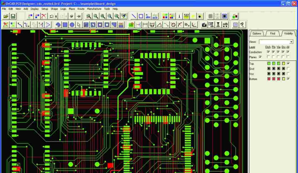
Learn the Design Software
Mastering PCB design tools takes time and practice. Work through documentation and video tutorials to become proficient with:
- Schematic capture – Drawing circuit diagrams with components and nets
- Component libraries – Adding desired logic ICs, discretes, connectors
- Board shape and layers – Defining board outlines and layer stackup
- Placement – Positioning components on the board canvas
- Routing – Drawing PCB traces to connect component pads
- Design rules – Configuring manufacturing constraints like trace width
- 3D modeling – Visualizing the populated board in 3D for clearance checking
- Generating outputs – Producing Gerber, drill, and pick-and-place files
As skills improve, efficiency with the toolset increases.
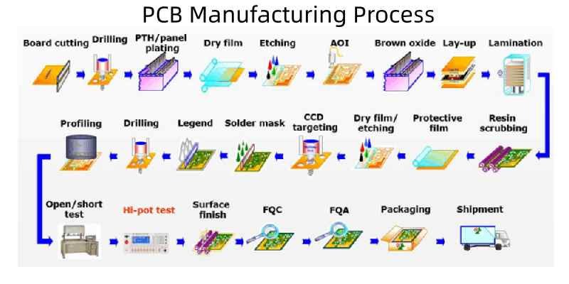
Learn PCB Manufacturing Processes
Understanding how PCBs are fabricated ensures designs are manufacturable. Key processes to understand:
- PCB Layer Stackup – Materials used for layers and why
- Lamination – Fusing layers under heat and pressure
- Drilling – Machines used to drill component holes
- Imaging – Photoresist coating for conductor patterning
- Etching – Removing copper not protected by resist
- Plating – Electroplating boards for conductivity and solderability
- Solder mask – Protective epoxy layer over traces
- Silk screen – Printed labeling layer
- Surface finishes – ENIG, immersion silver, OSP, etc.
- Via formation – Processes for creating plated through hole interconnects
- Routing and scoring – Singulation into individual boards
Considering capabilities and limitations of manufacturing processes helps optimize designs.
Learn Key Design Principles
Applying sound design principles ensures PCBs function reliably. Key concepts include:
- Component placement – Group related sections, minimize wire lengths
- Routing – Use adequate trace widths, minimize vias and crosses
- Decoupling – Use proper decoupling capacitors for each IC
- Impedance control – Match trace impedance to device requirements
- Thermal management – Ensure components get adequate airflow and cooling
- Current capacity – Use adequate copper weights for power traces
- Grounding – Provide robust ground plane return paths
- Signal integrity – Control noise, cross-talk, and impedance mismatches
- Redundancy – Include backup options for critical paths like clocks
Adhering to best practices leads to robust, quality PCB designs.
Create a Small First Project
An excellent way to apply skills is starting out by designing a simple board like:
- Development board – For a small microcontroller or single-board computer
- USB-powered device – Such as hobby gadget with buttons and LEDs
- Sensor board – For interfacing a few sensors to a microcontroller
- Carrier board – To plug in an application-specific integrated circuit (ASIC)
- Clock module – Digital clock powered by microcontroller
Don’t attempt overly complex designs initially. Keep the component count low and focus on fundamentals.
Have PCBs Manufactured
There are many low-cost options for prototyping through fabrication services like:
- PCBWay – Low volumes and quick turnaround
- RAYPCB – PCB Manufacturing and Assembly
- JLCPCB – Inexpensive boards with minimum 2-layer option
- OSH Park – Domestic US service with high quality
- ALLPCB – Multilayer boards with online checks before ordering
- Aisler – Specializes in manufacturing small quantity
Review design rules and get quotes before ordering. Hands-on lessons emerge once boards are in hand.
Test and Iterate
Always test assembled boards thoroughly:
- Verify there are no manufacturing defects or missing components
- Check power and grounds are properly connected
- Test sub-circuits incrementally before full integration
- Validate I/O drivers and receivers using an oscilloscope
- Program firmware and run through operational tests
- Make revisions to correct issues in the next design revision
Good designs take several prototyping iterations before reaching maturity. With each version, capabilities improve.
Expanding PCB Design Skills
Some additional ways to accelerate at PCB design include:
- Studying schematics and layouts of open source projects
- Reading application notes and reference designs for components you use
- Trying a more advanced design software tool like Altium
- Learning relevant simulation, signal integrity, and EMI analysis software
- Understanding design for manufacturing (DFM) principles and design rules
- Attending trade conferences and taking specialized training classes
- Getting formal education in electrical engineering and electronics
- Seeking mentorship from experienced hardware engineers
PCB design mastery demands continual learning and development.
An Empowering Skill Set
The ability to translate a circuit concept into a physical PCB design that works as intended is an immensely empowering engineering skill. PCB design unlocks the capacity to invent completely new devices. With some dedicated effort to learn the fundamentals, beginners can get started designing their own boards and making their electronics ideas physical.
FQA
What are some beginner circuit concepts and components to learn about for PCB design?
As a new PCB designer, study basic circuits using resistors, capacitors, transistors, logic gates, microcontrollers, voltage regulation, button/LED interfaces, and communications like I2C and SPI.
What are the main differences between low-cost and professional PCB design software tools?
Low-cost tools allow learning fundamentals but often lack advanced capabilities for signal integrity analysis, thermal modeling, manufacturability checks, and team collaboration features expected in professional tools.
What are some key factors to consider when selecting a PCB fabrication service?
Evaluate capabilities (layers, features), service (lead time, order quantities), quality (reliability), and costs (pricing model). Align choices with project needs.
How can studying open source hardware help when learning PCB design?
Observing schematics and PCB layout techniques used in open projects accelerates learning. Seeing solutions helps internalize design approaches faster.
What electronics and engineering knowledge is most valuable for professional PCB designers?
Firm grasp of digital/analog electronics, schematic capture, component libraries, layout/routing, manufacturability, design analysis, DFx skills, and communication ability enables effective professional board design.


