Introduction
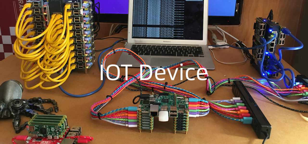
The Internet of Things (IoT) is transforming the way we live and work by connecting physical objects and devices to the internet and enabling them to send and receive data. IoT devices like smart home appliances, wearables, industrial sensors, and automotive telematics contain hardware and software that allow them to sense, compute, and communicate.
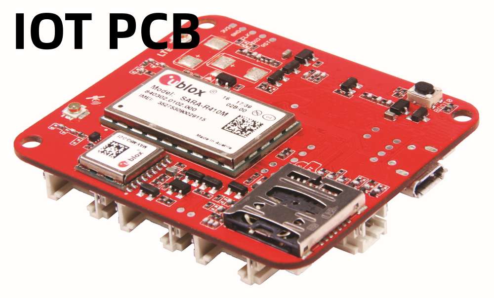
At the heart of any IoT device is the printed circuit board (PCB) which serves as the foundation for the components that enable IoT functionality. PCB design is an essential part of engineering IoT products. It requires consideration of the device’s capabilities, target environment, power requirements, manufacturability, and other factors.
This comprehensive guide will walk you through the end-to-end PCB design process for an IoT device using best practices at each step.
Define Requirements and Specifications
The first step is to clearly define the requirements and specifications for your IoT device based on its intended use and capabilities.
Consider parameters like:
- Sensors and peripherals – What kind of sensors, I/O interfaces and peripherals are needed? e.g. temperature sensor, accelerometer, Bluetooth/Wi-Fi module, antenna etc.
- Processing power – Will an MCU or processor be required for local computing and decision making?
- User interface – Are elements like LCD displays, LEDs, buttons, or buzzers needed for user interaction?
- Communication protocols – What wireless communication protocols will the device use e.g. Wi-Fi, Bluetooth, Cellular etc?
- Power requirements – What is the voltage and current requirement? Will the device be battery operated or AC powered?
- Physical specifications – What are the constraints on device size, shape, weight and operating temperature range?
- Security considerations – Does the device need measures like authentication and encryption to protect against cyberthreats?
- Costs – What are the cost constraints for the bill of materials (BOM) and total unit cost?
Documenting detailed, quantifiable requirements will guide PCB design decisions later on.
Select Key Components
Once requirements are clear, the next step is to select the key components that will be used in the design. These usually include:
Microcontroller (MCU) or Microprocessor
This is the brain of the IoT device that processes data and controls peripherals. Popular choices include Microchip’s AVR and ARM-based MCUs, STMicro STM32, Espressif ESP32, etc.
The MCU selection depends on processing power, speed, memory needs, operating voltage, cost, development tools availability and power consumption.
Communication Modules
Most IoT devices need to transmit and receive data wirelessly using protocols like Wi-Fi, Bluetooth, LoRa, NB-IoT or Sigfox. Choose modules that integrate the transceiver chip, antenna and other components into a single package.
Consider range, bandwidth, power consumption, form factor and cost when selecting wireless modules.
Sensors
The sensors in an IoT device gather environmental data like temperature, motion, humidity, proximity, etc. Choose sensors that provide sufficient accuracy and resolution for the application.
Look at power consumption, interface type (analog, I2C, SPI), and package when selecting sensors.
Peripherals and User Interface
Additional components like displays, buttons, speakers and LEDs may be needed for user interaction. Connectivity peripherals like USB and ethernet ports may be required for wired communication.
Select standard connectors and packages that integrate well with the form factor of your device.
Power Supply
Determine the appropriate voltage rails and energy source i.e. battery or adapter. Select supporting components like regulators and supervisory circuits.
Design the Circuit Schematic
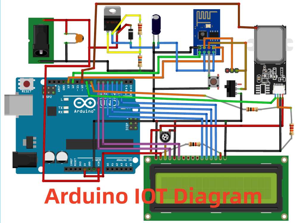
With the key components selected, the next step is to design the circuit schematic. This is the logical diagram showing the electrical connectivity between all components on the board.
Use CAD software like Altium Designer, Eagle, OrCAD or KiCad for schematic design.
Here are some best practices for IoT schematic design:
- Clearly indicate all ports and pins for each component. Provide descriptive names.
- Group related components together for better readability.
- Add test points to facilitate debugging and testing.
- Show all power connections, decoupling capacitors and voltage regulators.
- Include a crystal oscillator circuit for generating clock signals if required.
- Add programming and debug interfaces like SWD or JTAG for firmware programming.
- Include protection devices like LED drivers, fuses and ESD protection as needed.
- Create hierarchical sheets for complex sub-circuits and show key signals between sheets.
The schematic should be complete with all connectivity and components required for functioning of the IoT device. Follow conventions for readability.
Lay Out the PCB
With the circuit schematic completed, the next major step is PCB layout using PCB design software. This involves:
1. Placing Components
Place components strategically based on connections to optimize routing, thermal considerations and manufacturability. Place connectors, indicators and any sensitive RF circuitry first.
Group related sections together. Leave adequate space between components for routing.
2. Routing the Traces
Interconnect the pins and ports of each component with copper traces based on the schematic connectivity. Maintain short, direct traces for critical signals like clocks and analog signals. Keep high speed traces away from noisy paths.
Use wide traces and polygons for power distribution. Include vias for connections between layers.
3. Completing the Board Outline
Draw the physical board outline, cutouts and drill holes. Ensure the size matches the specified form factor. Include any required mounting holes.
4. Adding Text and Other Details
Add reference designators, layer names and other text markings. Include any logos, ratings and legal labels. Add dimensioning, fabrication notes and documentation.
Run design rule checks and manual verification to ensure manufacturability. Make any required tweaks at this stage before finalizing the board layout.
Select the Right PCB Materials
PCB substrate choice can impact cost, manufacturability and device performance. Consider factors like:
- Number of layers – 2 to 6 layer PCBs are commonly used for IoT devices depending on complexity.
- Board thickness – Typically between 1.6 mm to 2.4 mm. Thicker boards provide more rigidity.
- Material – FR-4 is the most common PCB material. High frequency boards may require RF substrates.
- Copper thickness – 1oz (35 μm) copper is standard. 2oz or 3oz copper may be used for higher current capacity.
- Coating – Mask, silkscreen and solder mask should be selected based on aesthetics, insulating requirements and visibility of markings.
- Special finishes – Immersion silver, ENIG or HASL PCB surface finishes can improve solderability and contact resistance.
Discuss specific requirements with your PCB manufacturer early in the design flow.
Simulate and Validate the Design
Before fabricating the PCB prototype, the design should be thoroughly simulated and validated:
- Run signal integrity simulations using HyperLynx or Ansys SIwave to verify high speed signals.
- Perform power integrity analysis with HyperLynx PI or Ansys RedHawk to check power distribution.
- Use thermal simulation using tools like Icepak or FloTHERM to identify any hotspots.
- Validate manufacturability using design rule checks.
- Perform electromagnetic interference (EMI) and radio frequency (RF) analysis as needed.
- Review the design data against requirements.
Simulation provides insight into any issues or bottlenecks in the design before manufacture.
Fabricate and Assemble Prototype Boards
Once the design is finalized, low volume prototype PCBs can be fabricated from vendors that support quick-turn fabrication to build the first batches.
Carefully inspect the bare PCBs for any defects, missing markings or drilling issues. Test key parameters like insulation resistance and impedance of critical traces.
After bare board validation, assemble a prototype by soldering components either manually or through an assembly service. Use adequate ESD precautions.
Inspect for any missed joints, bridging or component placement issues. Functionally test the prototype by powering it up and verifying communication, sensor data and other functionality.
Debugging and refinement of the PCB and firmware may be needed over several revision cycles before design freeze and mass production.
Key PCB Design Guidelines for IoT Products
Here is a summary of some key PCB design guidelines and best practices for robust, reliable and cost-effective IoT hardware:
- Optimize component placement for compactness, considering proximity of connected sections.
- Provide adequate thermal reliefs and heat sinks if high power dissipation is expected.
- Include test points, programming and debug provisions for easy troubleshooting.
- Maintain controlled impedance for traces carrying high speed data.
- Use wider traces and polygons on inner layers for power distribution.
- Design with manufacturing and assembly in mind. Allow sufficient tolerances and spacing.
- Reduce analog circuit noise through isolation, shielding and filtering.
- Verify critical parameters through simulation during the design stage.
- Validate PCB performance under expected environmental conditions.
- Work closely with fabrication and assembly partners to avoid manufacturability issues.
Adhering to these guidelines will help accelerate the design process and reduce risks as you develop the key hardware for your IoT product.
IoT PCB Design Considerations – Frequently Asked Questions
Here are some common questions around designing PCBs for IoT devices:
Q1. How can I reduce the BOM cost in an IoT PCB design?
A1. Some ways to lower BOM cost for an IoT PCB:
- Design the board to eliminate unnecessary components.
- Select lower cost versions for peripherals like sensors and connectors with acceptable performance.
- Use common, high volume components as much as possible.
- Minimize number of unique part numbers. Reuse components wherever possible.
- Work with vendors to negotiate better pricing for high quantity orders.
- Consider older generation ICs which may have lower cost.
- Use QFN/DFN packages instead of larger LQFP packages to reduce size and cost.
Q2. What can impact an IoT product’s time to market during development?
A2. The key factors impacting time to market during IoT product development are:
- Completeness of requirements – Inadequate upfront planning can cause rework.
- Simulation and prototyping time – Insufficient testing can delay design validation.
- Timely decision making – Slow component selection and design choices delays the process.
- Manufacturing cycle time – Long fabrication and assembly lead times.
- Software development timeframe – Integrating hardware with firmware/cloud adds schedule time.
- Regulatory testing and certification timeline – Mandatory for commercial release.
- Time taken for rounds of debugging and design refinement based on prototype test results.
Q3. What are some best practices to make an IoT PCB design more reliable?
A3. Some reliability best practices for IoT PCB design are:
- Select robust, automotive-grade or industrial temperature range components.
- Use redundant backup components like supervisory circuits and watchdogs.
- Include voltage protection devices like transient voltage suppressors.
- Design for mechanical rigidity – avoid thin/flexible sections.
- Conformally coat the PCB assembly to prevent corrosion.
- Validate design over required environmental conditions (temp., vibration, shock etc).
- Analyze thermal performance to avoid hot spots.
- Ensure robust power supply design with adequate filtering.
- Follow design for manufacturability (DFM) guidelines to prevent field failures.
- Test prototype thoroughly through HALT (highly accelerated life testing).
Q4. How can EMI/EMC issues be minimized in an IoT PCB design?
A4. Some ways to minimize EMI/EMC issues in IoT PCB design:
- Use shielding enclosures for sensitive analog and RF circuits.
- Include metal/graphite gaskets between mating surfaces of enclosure.
- Use common ground planes. Minimize ground loops. Provide multiple layer-to-layer ground vias.
- Isolate noisy digital circuits from sensitive analog sections.
- Use bypass/decoupling capacitors near every IC to filter noise.
- Add ferrite beads and other passive filter components on I/O lines.
- Keep high speed trace lengths short. Use controlled impedance routing.
- Avoid slots/cutouts on ground planes below critical traces.
- Validate EMI and susceptibility through pre-compliance testing.
Q5. How can manufacturability of an IoT PCB be improved?
A5. Some ways to improve manufacturability of an IoT PCB design:
- Allow adequate spacing between components and keepouts for routing channels.
- Ensure design complies with board house fabrication capabilities.
- Avoid traces between closely spaced pads or vias.
- Use standard thickness PCB materials. Minimize special requirements.
- Keep high density sections limited to areas with less routing congestion.
- Review soldermask defined vs. non soldermask defined pad layouts.
- Minimize component placements requiring reflow process on both sides.
- Use simpler rectangular board outlines where possible.
- Clearly specify special PCB finishes, tolerances, colors and material requirements.
- Specify widely available components and packages.
- Run design rule checks and discuss with manufacturers.
Conclusion
Designing optimized, robust and cost-effective PCBs is crucial to developing successful IoT products. Careful requirement analysis, component selection, schematic design, PCB layout, simulation, prototyping and testing helps get the hardware design right. Keeping manufacturing considerations in mind and collaborating closely with supply chain partners also accelerates the development cycle. Applying the guidelines outlined in this article will help you maximize the value delivered by your IoT system while minimizing time to market.


