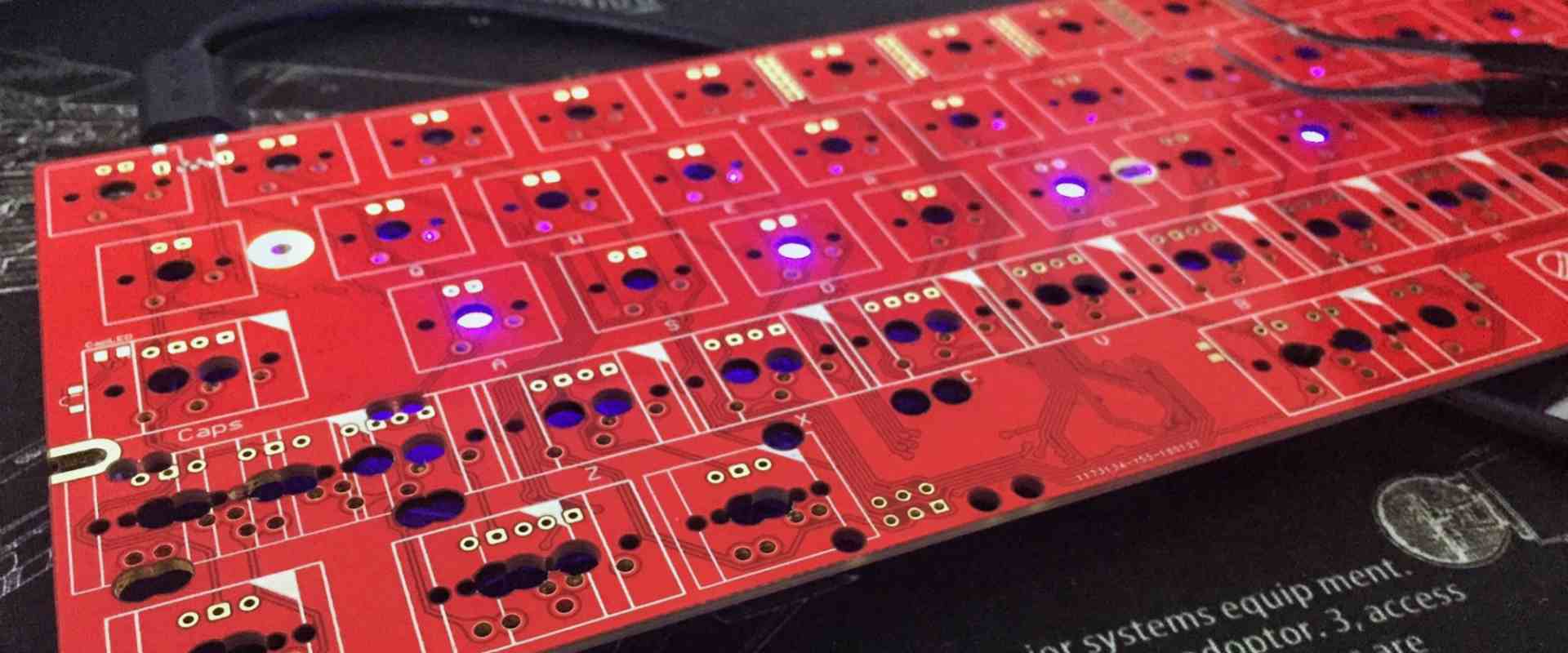
A keyboard PCB (printed circuit board) is the main internal component of a computer or electronic keyboard that houses the circuitry and connections for all the keys. This article provides an overview of keyboard PCB types, manufacturing processes, design considerations, and cost factors.
What is a Keyboard PCB?
A keyboard PCB serves as the underlying platform to mount all the components and circuitry that allow a keyboard to register key presses and communicate them to a host device.
The main elements of a keyboard PCB include:
- Traces to connect each individual key switch to a keyboard microcontroller
- Traces for power distribution
- Mounting points for the key switch mechanical plate
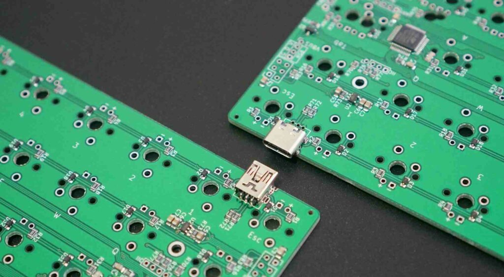
- Connectors for wiring to connect to the computer/device
- Mounting areas for any additional components like LEDs, resistors, diodes etc.
The PCB provides the structural base and electrical connections that allow assembling all parts into a working keyboard.
Types of Keyboard PCBs
Keyboard PCBs can be categorized based on a few key criteria:
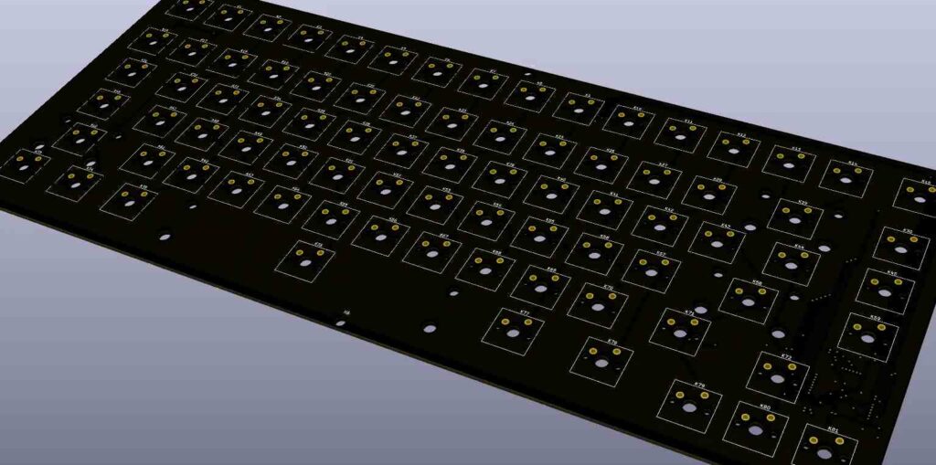
1. Layout
- Full-size: Supports all standard keys including numeric keypad (~104 keys)
- Tenkeyless (TKL): Removes numeric pad (~87 keys)
- Compact: Further reduced layouts removing navigation keys etc.
2. Layers
- Single-sided: Traces on only one side
- Double-sided: Top and bottom layer traces
- Multi-layer: 4-16 layers stacked for complex routing
3. Switch Mounting
- Plate mount: Switches clipped onto a metal plate first
- PCB mount: Switches mount directly onto the PCB
4. Customizability
- Pre-designed: Fixed layout with minimal configurability
- Modular: Sections that allow layout rearrangement
- Fully Custom: Blank PCB for any layout
There are also unique PCBs designed for low-profile, optical, ergonomic and other special keyboard mechanisms.
Keyboard PCB Design Considerations
Designing a keyboard PCB requires careful planning for the following:
1. Layout
The size, shape and placement of keys and additional components is crucial. Allows keys to be logically placed and routed.
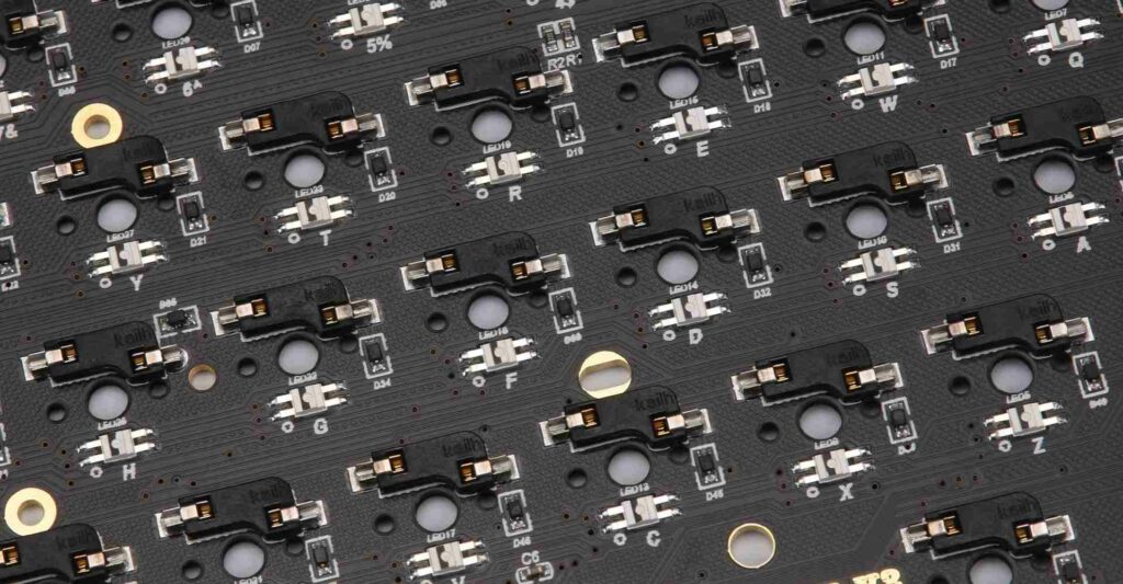
2. Switch Matrix
The electrical network of rows and columns wired to the keyboard switches. Impacts how many keys can be independently sensed.
3. Controller
An MCU or chip that reads the switch matrix and sends keypress data to host. Must support required features.
4. Electrical Rules
Follow stringent PCB design rules and guidelines provided by the PCB manufacturer for reliable fabrication.
5. EMI and ESD Protection
Add components to prevent electromagnetic interference and electrostatic discharge issues.
6. Cost and Manufacturability
Design considerations to optimize board cost like layers used, complexity, size etc.
Careful keyboard PCB design is key to creating a robust, reliable and quality end product.
Keyboard PCB Manufacturing Process
Modern keyboard PCBs are fabricated using automated industrial-scale PCB manufacturing processes. Here are the key steps:
1. Design
The PCB layout is designed in EDA software like Altium, Eagle, KiCad etc. which generates Gerber files.
2. Solder Mask Layer
A solder mask layer is added to prevent solder bridging between pads during assembly.
3. Silkscreen Layer
Legend and markings are added using the silkscreen layer for easy identification.
4. Surface Finish
A chemical layer like HASL, immersion gold, ENIG etc. is added for solderability and protection.
5. Automated Assembly
Components are placed and soldered using pick-and-place and reflow/wave soldering.
6. Testing and QC
100% electrical testing using fixtures to validate all connections and functionality.
7. Packaging
Boards are packed with ESD protection for shipping to customers.
Specialized PCB factories offer one-stop manufacturing capabilities for professional keyboard products.
Design Tips for Keyboard PCBs
Here are some tips for optimizing keyboard PCB design:
- Use a minimum of 2 layers for cleaner routing, better aesthetics.
- Include generous clearance around switch holes for stability.
- Place controller centrally with balanced layout to simplify routing.
- Use surface mount components to avoid drill holes weakening the board.
- Add reinforcement by increasing copper amounts in heavily used areas.
- Rotate adjacent keys by 90 degrees to minimize interference.
- Ensure switch hole spacing matches plate spacing precisely.
- Reduce trace length mismatches to improve signal integrity.
- Include status LEDs aligned with switch holes for visibility.
- Add descriptive silkscreen labels next to connectors.
With careful engineering and testing, high quality and reliable keyboard PCBs can be designed cost-effectively.
Keyboard PCB Cost Considerations
The total cost of a keyboard PCB involves several elements:
NRE and Tooling Costs
- NRE charges for initial engineering and design.
- Tooling costs for fabricating masks and test jigs.
PCB Fabrication Cost
- Number of layers and complexity impacts cost per board.
- High-end PCB materials drive up cost.
- Advanced manufacturing capability required also adds cost.
Component Costs
- Keyboard controllers, switches, connectors have varying price points.
- Higher pin count controllers cost more.
- Number of LEDs, diodes and other parts impact BOM cost.
Assembly Cost
- Automated SMT assembly has rate based on number of parts.
- Manual assembly or minor rework adds cost.
Testing and Certification
- Test fixture development required for quality control.
- Certifications like UL, FCC etc. add compliance costs.
Quantity and Size
- Smaller quantities have higher cost per board.
- Miniaturization requires more layers and Density costs.
Cost Saving Tips
Ways to reduce keyboard PCB costs:
- Use simpler single/double layer PCBs where possible.
- Choose lower pin count controllers.
- Reduce number of cosmetic LEDs.
- Stick to standard shapes and sizes to avoid NREs.
- Order larger quantities for volume discounts.
- Use pre-certified components to avoid re-certification.
- Consider assembly in lower-cost regions.
- Reuse tooling like test jigs across keyboards.
- Work with vendors to identify cost reduction opportunities.
- Compromise on advanced PCB materials/finishes if possible.
Example Cost Breakdown
Here is an indicative cost breakdown for a sample full-size 104 key keyboard PCB with RGB backlighting:
| Item | Estimated Cost |
|---|---|
| PCB Fabrication (2-layer) | $5 |
| Switches (104) | $40 |
| Keycaps | $20 |
| Controller | $3 |
| Stabilizers | $2 |
| Other Components | $6 |
| PCB Assembly | $4 |
| Packaging and Handling | $2 |
| Total Cost per Unit | $82 |
This demonstrates typical keyboard PCB cost components. Significant variation is possible based on design decisions.
Conclusion
- The PCB provides the electrical backbone connecting all components inside a keyboard.
- Many design factors like layout, switch matrix, controller, manufacturability etc. must be considered.
- Industrial scale automated PCB fabrication and assembly enables cost-effective keyboard manufacturing.
- Cost optimization should balance BOM reduction and quality to meet end-user pricing targets.
Top 5 FAQs about Keyboard PCBs
Q1: What are the main components on a keyboard PCB?
The most important components are the controller IC, electrical switch matrix,keycap LEDs, and cable connectors.
Q2: What CAD tools do keyboard designers use?
Most common tools are Eagle, KiCad and Altium for schematics and PCB layout. Some use web-based PCB design platforms.
Q3: How are components mounted onto the PCBs?
SMT assembly is used to place tiny SMD parts. Switches and connectors use through-hole mounting or are attached to the mechanical plate.
Q4: How many layers are optimal for keyboard PCBs?
2 layers suffice for standard keyboards. More complex routing requires 4-6 layers. High-end keyboards may use up to 16 layers.
Q5: Can existing keyboard PCBs be customized?
Yes, open-source keyboard PCB designs can be modified and redesigned to create custom layouts and features.


