Introduction
Flexible printed circuit boards (flex PCBs or flex circuits) are a type of printed circuit board that is made of flexible insulating substrate materials such as polyimide or polyester. Unlike rigid PCBs, flex PCBs can be bent and folded to fit into tight spaces and movable parts. They are commonly used in consumer electronics, medical devices, industrial equipment, and aerospace applications where flexibility, durability and space savings are required.
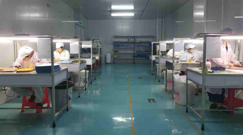
The manufacturing process of flex PCBs involves many steps including design, fabrication, assembly, and testing. While the fabrication process shares similarities with rigid PCB fabrication, additional steps are required to handle the flexible materials involved. Understanding the flex PCB manufacturing process is important for designing and producing high quality and reliable flex circuits. This article provides an overview of the major steps involved in manufacturing flexible printed circuit boards.
Flex PCB Design
The design process lays the groundwork for manufacturing by defining the circuit layout and electrical connections. Here are some key design considerations for flex PCBs:
Circuit Layout
- The arrangement of conductive traces, components and other features on the PCB. Flex circuits can have complex geometries with folds, bends and branches.
Stackup
- Selecting the number of conductive layers and the materials used for dielectric layers, covers, stiffeners, adhesives. Common materials are polyimide, acrylic, polyester.
Copper Thickness
- Thinner copper (1/2 to 1oz) is typically used to maintain flexibility. Thick copper may be used in high current areas.
Conductor Width and Spacing
- Narrower traces with finer spacing are needed for high density flex PCBs.
Bend Radius
- Minimum bend radius requirements based on materials used to prevent damage.
Vias and Holes
- Used to connect layers and mount components. Special consideration for reliability of plated through holes (PTHs) in dynamic flexing conditions.
Stiffeners and Covers
- Added for protection, rigidity and ease of assembly.
Fabrication Data
- Additional details for manufacturing such as outline, cut lines, tooling holes.
Careful flex PCB design is important to avoid issues during manufacturing and assure reliability in the end product.
Flex PCB Fabrication Process
The fabrication process transforms the PCB design into a physical circuit board. Here are the key fabrication steps:
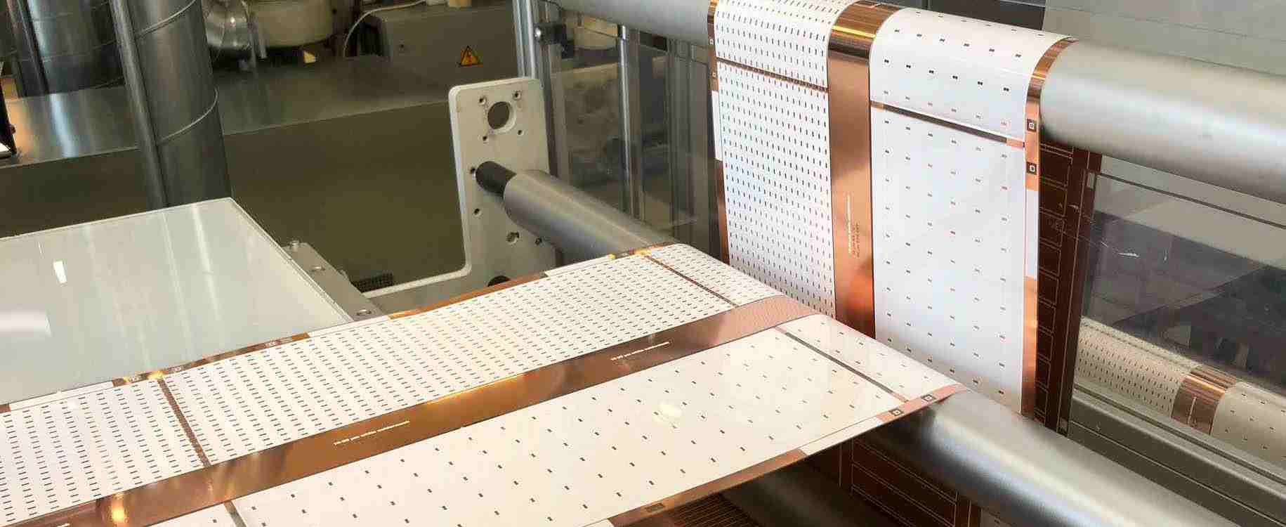
1. Copper Foil Lamination
The process starts with bare copper foil which will form the conductive layers. The foil is cleaned and coated with an adhesion promoting chemical. Layers of dielectric material (polyimide, polyester, etc) and copper foils are stacked up and precisely aligned. The stackup goes through a lamination press under heat and pressure to bond the layers together into a solid board.
2. Imaging
A photosensitive dry film is laminated onto the copper surfaces. The film is exposed to UV light through a mask patterned with the circuit layout. This transfers the pattern to the film. Unexposed areas of the film are then dissolved away. This forms a protective layer over the copper that will remain after etching.
3. Etching
The board is passed through an etchant solution, typically ammonium persulfate or ferric chloride. This chemically dissolves and removes the unprotected copper, leaving only the desired circuit pattern.
4. Photoresist Stripping
The remaining dry film is stripped away using a chemical solution, revealing the full conductive pattern on the board.
5. Hole Drilling
Holes are mechanically drilled or punched through the board to form vias for layer interconnections and component mounting. Precise location and size of the holes is critical.
6. Plating and Coating
Surfaces are prepared and cleaned. Conductive layers and hole walls are plated with copper to desired thickness. Protective coatings such as solder mask and gold plating are selectively applied over conductors and contact fingers.
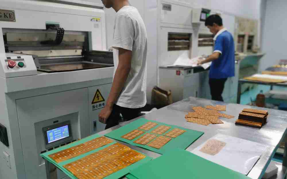
7. Trimming and Shaping
The fabricated PCB panel is cut to remove excess material and cut into individual boards or arrays. Additional processes like contour milling and 3D shaping may be used to form complex flex board shapes.
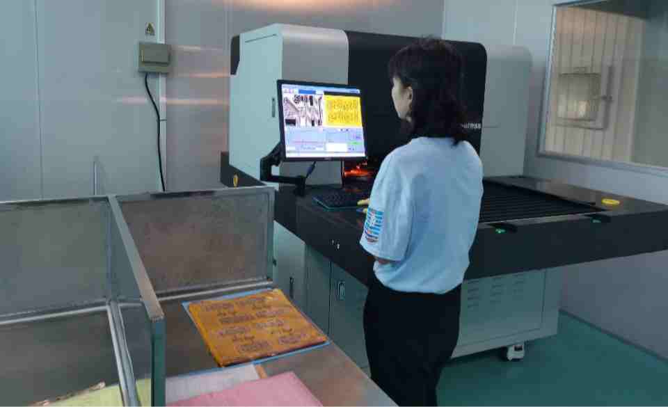
8. Electrical Testing
Each board undergoes electrical testing to verify connectivity, isolate defects, and ensure the fabrication meets specifications. Testing methods include flying probe, bed of nails, and automated optical inspection.
9. Final Finishing
Additional steps like legend printing, edge trimming, and corner chamfering are done to complete the boards. Cleaning and protecting the flex boards from damage completes the fabrication process.
Flex PCB Assembly
After fabrication, assembly of components and connectors is required to produce finished flex circuit assemblies:
1. Solder Paste Printing
Solder paste containing metal alloy powder and flux is printed or dispensed onto substrate pads. Stencils or screens are used to accurately deposit the paste.
2. Component Placement
Components are precisely picked and placed onto the solder paste deposits using automated assembly machines.
3. Reflow Soldering
The assembly enters a reflow oven. The temperature profile melts the solder paste to form solder joints that attach and electrically connect the components.
4. Conformal Coating
A protective coating may be selectively applied over the assembly, covering components and solder joints. It protects against environmental threats like moisture and abrasion.
5. Attachment
Additional parts, housings, connectors and other items are mechanically attached to complete the flex circuit assembly using methods like soldering, adhesion and press-fitting.
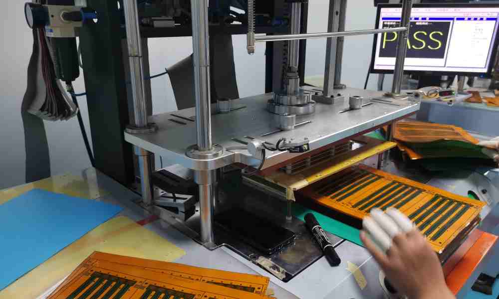
6. Final Testing
Electrical testing and inspection verifies the quality and functionality of the completed assembly. Parameters like continuity, insulation resistance and dielectric strength are measured.
Flex PCB Testing and Quality Control
Maintaining quality control throughout the manufacturing process is crucial for reliability:
- Raw materials are qualified and process controls are implemented to ensure consistent quality.
- At multiple steps like drilling, plating and etching, dimensions and thickness are verified. Optical inspection tools may be used.
- Test coupons with dedicated test traces are fabricated and measured to monitor parameters like adhesion, resistance and insulation breakdown.
- Before assembly, boards undergo electrical testing to catch any fabrication defects or damage.
- During assembly, components are inspected, tested and boards monitored to catch errors early.
- Final testing on completed assemblies stresses and verifies the design’s electrical performance and long term reliability under bending and other environmental conditions.
With close monitoring and testing at each process step, any defects or issues can be quickly identified and corrected. This prevents problems from progressing further and impacting downstream processes.
Common Tests for Flex PCBs
| Test | Description |
|---|---|
| Electrical Testing | Checks conductivity, insulation resistance and dielectric breakdown |
| Mechanical Testing | Bend radius, twist, vibration, shock tests |
| Environmental Testing | Performance in humidity, temperature cycling, etc |
| Reliability Testing | Dynamic bending, torsion, operation life tests |
Benefits of Flex PCBs
Understanding the manufacturing process helps appreciate the advantages of flex PCB technology:
- Complex layouts – Multi-layer circuits with high density traces can be fabricated.
- Dynamic flexing – Withstand repeated bending without conductors cracking.
- Light weight – Thin, flexible materials instead of rigid glass-epoxy boards.
- Space savings – Can tightly fit and integrate into products.
- Reliability – Robust performance in vibration, impact and varying temperatures.
- Design freedom – Enable flexible, moving and compact electronic devices.
Flex PCB Manufacturing FAQs
Q: How is impedance controlled on flex PCBs?
A: Maintaining consistent impedance requires careful control of trace dimensions, dielectric material properties and layer stackup. Thinner dielectrics with lower permittivity allow higher impedance traces. Wider spacing between traces also increases impedance. Stripline traces between ground planes give better impedance control than microstrip configurations.
Q: What are some key tests conducted on flex PCBs?
A: Electrical testing checks conductivity, insulation and dielectric breakdown. Mechanical tests like bend radius, twist, vibration and shock determine robustness. Environmental tests verify performance in humidity, temperature cycling and other conditions. Reliability testing stresses dynamic bending, torsion and operation life.
Q: How are components assembled on flex circuits?
A: SMT components are applied with solder paste and reflow soldering. Selective conformal coating may be used. Larger components use solder, conductive epoxy or mechanical attachment. Careful handling is needed as flex boards are more fragile than rigid PCBs during assembly.
Q: What materials are used for flexible PCB substrates?
A: Polyimide films like Kapton are most common. Others include polyester (PET), polyetheretherketone (PEEK), polyetherimide (PEI), polycarbonate, polyvinyl chloride, Teflon and polyethylene. Material selection depends on flexibility, temperature and electrical requirements.
Q: How does flex PCB fabrication differ from rigid PCBs?
A: Additional steps for lamination and bonding of thin flexible layers are required. Etching, drilling and plating processes need to accommodate flexible boards. Handling, carriers and cover sheets help prevent stretching or distorting flex materials during fabrication.
Conclusion
Flexible PCB manufacturing combines processes adapted from rigid PCB fabrication with innovations that enable the use of thin, heat-resistant flexible materials. The result is robust circuits that can take on complex 2D and 3D shapes ideal for modern electronic devices. An understanding of the design considerations, specialized fabrication steps, assembly methods and testing procedures involved gives important insights into realizing high quality flex circuits. Continued advancements and cost reductions in flex PCB technology will enable their expanded use and drive development of the next generation of flexible, wearable and internet-connected products.


