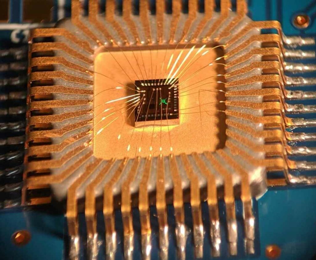
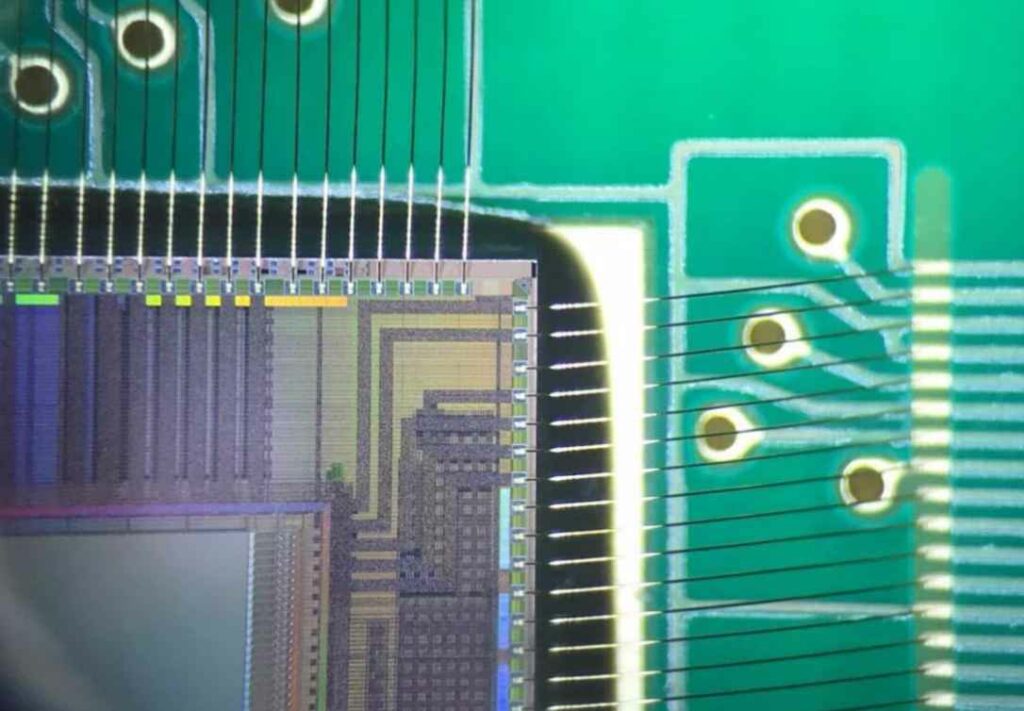
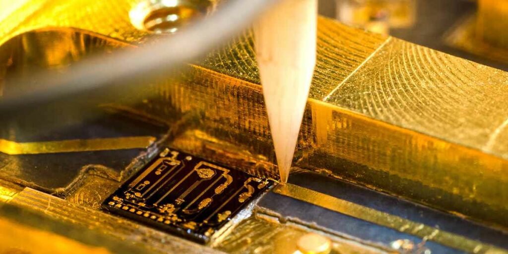
In electronics, wire bonding is a method used to electrically connect semiconductor dies or chips to external circuitry like package leads or printed circuit boards (PCBs). It involves using very fine wires to make interconnections between pads on the die to the pads on the substrate or lead frame it is being assembled on.
Wire bonding is an essential part of semiconductor device packaging and PCB assembly. It enables reliable connections from the microscopically small pads on silicon chips to the much larger pads and traces on packages and circuit boards. Understanding wire bonding is important for anyone involved in electronics manufacturing.
This article provides a detailed overview of wire bonding, its role in PCB assembly, the different wire bonding techniques, bond types, equipment used, and advantages versus other interconnection methods.
Role of Wire Bonding in PCBs
While often associated with semiconductor packaging, wire bonding also plays an important role in many PCB assemblies. Reasons wire bonds are used on PCBs include:
- Connecting IC dies directly onto the board, called chip-on-board mounting.
- Interface connections for installing packaged ICs onto boards, like connecting leads.
- Making repairs to damaged PCB traces by bridging gaps with wire bonds.
- Prototyping circuits by manually connecting components with wires before soldering.
- Attaching connectors like FFCS and RF modules that use wire bonding pads.
- Providing more flexibility versus photolithographic traces on rigid boards.
So wire bonding facilitates the integration of various electronic components onto PCBs. The fine wires allow connections that would be difficult to achieve with etched metal traces alone.
Wire Bonding Techniques
There are two major techniques used in wire bonding – ball bonding that forms a ball bond, and wedge bonding that forms a wedge bond.
Ball Bonding
In ball bonding, a molten ball is formed on the end of the wire thread by an electronic flame off (EFO) process. The ball is pressed against the bonding pad while ultrasonic energy is applied along with force to deform the ball and create the bond. The ultrasonics break up the surface oxide enabling a metallurgical joint to be formed with the pad. After the ball bond, the wire is looped to the second bonding pad and another bond formed there by the same ball deformation process. The wire is then broken either via flame or mechanical clamping.
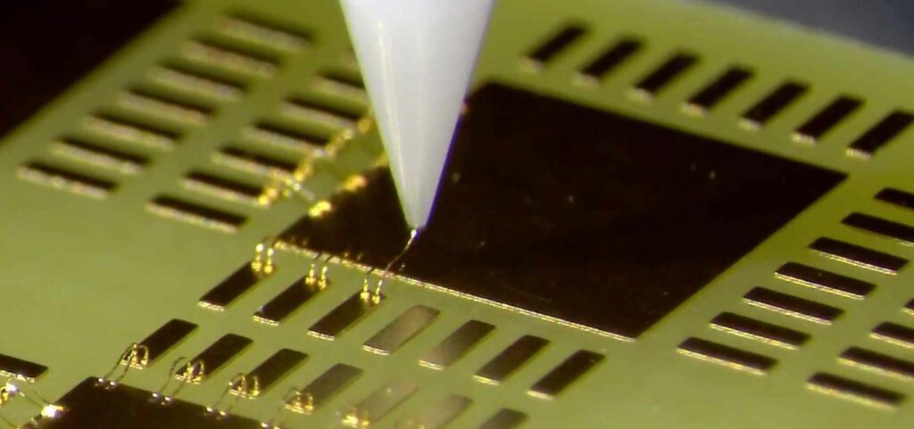
Wedge Bonding
In wedge bonding, the wire thread is pressed onto the bond pad surface while ultrasonic energy and force deforms and breaks up surface oxides on both the wire and pad. The wedge tool shapes the wire into its trademark wedge bond shape. Wedge bonding can use either a spool of bare wire feed or pre-formed wire loops. After making the first bond, the wire is looped to the second pad where another wedge bond is made, and then the wire is broken off.
Wedge Bonding Process (Image Credit: ResearchGate)
Both ball bonding and wedge bonding use combinations of heat, pressure, and ultrasonic energy to create reliable metallurgical wire-to-pad bonds. The main factors differentiating them are the bonding tool shape and resulting bond footprint.
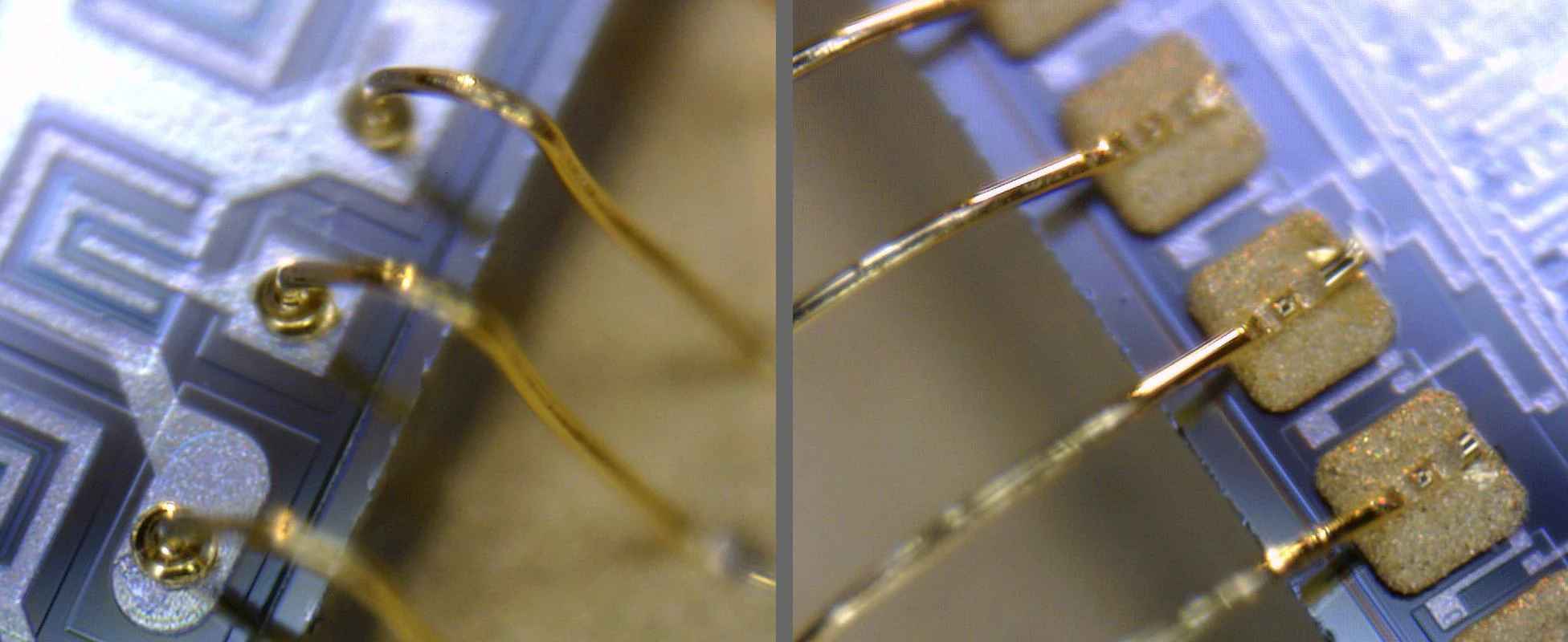
Wire Bonding Bond Types
Based on the area of contact between the wire and bonding pad, wire bonds are classified into two types – ball bonds and wedge bonds.
Ball Bonds
Ball bonds are created by ball bonding processes. The bottom of the wire ball engages an area of the pad equal to the cross-sectional area of the ball. This creates a bond with a circular footprint on the pad and a spherical protrusion rising above it. Ball bonds allow swooping high-loop wire trajectories in a confined space.
Wedge Bonds
Wedge bonds are created by wedge bonding processes. The side of the wedge tool compresses an area of the wire onto the pad surface to deform the wire into its wedge shape. This forms an elongated rectangular bond footprint on the pad. The low looping trajectory of wedge bonds allows them to be stacked closely together.
The shape of the bond affects the looping profile and spacing limitations between bonds, influencing the interconnection design.
Wire Bonding Materials
The materials used for wire bonding include:
- Bonding Wire – Typically gold, copper, aluminum or alloys, with diameters from 15 to 75 μm. Gold wire is most common due to excellent bondability. Copper and aluminum are lower cost alternatives.
- Bonding Pads – Usually aluminum or copper pads on chip or substrates, may have nickel, silver or gold plating. Compatible metallurgy between wire and pad enables bonding.
- Leadframes – Alloy 42 or copper leadframes are often wire bonded in packaging. Iron-nickel alloys are used for their similar expansion to silicon.
- PCB Traces – Copper traces on FR-4 boards can serve as bonding pads. May require gold plating or pretinning for bondability.
Proper material selection, pad metallization, and wire diameter optimize the wire bonding process for reliability and yield.
Wire Bonding Equipment
Wire bonding requires specialized equipment to precisely handle fine wires and create reliable bonds:
- Bonding Tool – For holding, feeding, shaping/deforming wires and applying ultrasonics. May be heated to assist bonding. Ball tool or wedge tool configurations.
- Workpiece Stage – High precision movable platform with bonding heat to hold chip/substrate. Provides bonding force and multi-axis positioning.
- Microscopes – Allows viewing bonded wires and precise alignment of tools to pads. Video systems provide enlarged visuals.
- Wire Payoff – Controls wire feeding from spool to bonding tool. Maintains proper wire tension and threading.
- Controllers – Sophisticated computerized control systems to drive the machinery and coordinate the bonding process.
- EFO System – For ball bonding processes, provides high voltage sparks to melt wire ends into balls and break bonds.
High throughput machines automate the entire wire bonding sequence for mass production. Some bond over 15,000 wires per hour.
Here is an overview of a typical automated wire bonding equipment system:
| Component | Description |
|---|---|
| Wire Spool | Supplies the spool of bonding wire mounted on the payoff system. |
| Wire Payoff | Feeds wire from spool maintaining proper tension. |
| Clamp | Secures wire during bonding. |
| Bonding Tool | Heated tool that presses, deforms and ultrasonically bonds the wire. |
| Bonding Stage | Heated platform that positions workpiece and applies bonding force. |
| Workpiece | Chip, substrate or PCB that bonds are formed on. |
| Microscope | Magnified visuals for aligning tool and inspecting bonds. |
| EFO System | Provides high voltage sparks for ball formation and bond breakage. |
| Camera | Video camera for enlarged microscope viewing. |
| XYZ Positioners | Allows precise positioning of tool, stage and workpiece. |
| Controller | Computerized system controlling all machinery parameters and bonding sequence. |
The integrated system provides the alignment accuracy and process control needed for reliable microscale wire bonding.
Wire Bonding Process Steps
While there are machine-specific differences, the general wire bonding process consists of these key steps:
- Setup – The workpiece is fixed in place on the heated bonding stage. The wire spool is loaded and threaded through the system. Tools are installed and calibrated.
- Ball Formation – For ball bonding, a ball is melted on the end of the wire protruding from the tool using an EFO spark.
- First Bond – The ball or wedge tool presses the wire onto the first bonding pad while heat, force and ultrasonic energy are applied to deform the wire and forge the metallurgical bond.
- Looping – The tool moves in the programmed looping trajectory to span between bonding sites as the clamp holds the wire stable.
- Second Bond – The tool presses onto the second bonding pad, forging another wire deformation bond with the applied heat, force and ultrasonics.
- Bond Break – For ball bonding, an EFO spark breaks the wire. For wedge bonding, the tool clamps to break the wire.
- Inspection – The completed wire bond is inspected visually or with other techniques like pull testing.
- Repeat – The process repeats with automatic indexing to subsequent bond sites across the workpiece until the bonding sequence is completed.
Precision movement of bonding tools and stages enables this sequence to be performed at very high speeds with reliability.
Wire Bonding Advancements
Some key advancements that have improved wire bonding processes over time include:
- Automation – Machines with computer numeric control have automated complex multi-pad bonding sequences and enabled mass production throughput.
- Vision systems – High magnification CCTV cameras and pattern recognition algorithms provide imaging-based feedback for superior bond placement accuracy.
- Plasma cleaning – In-situ atmospheric plasma units prepare bond surfaces just before bonding for consistently reliable bonds.
- Orthodyne technology – Allows both heavy and thin wire bonds to be made on the same machine by modulating ultrasonic power based on loop height.
- Ribbon bonding – Specialized for power devices, bonding heavy wires or strips of stamped ribbon instead of fine round wire.
- In-line monitoring – Sensors detect bond placement and pulling forces during the process for immediate yield feedback.
These improvements help achieve the yield, cost and reliability requirements of modern electronics manufacturing.
Wire Bonding Standards
To provide design guidelines and help assess bond quality, there are several industry standards related to wire bonding published by organizations like JEDEC, MIL-STD, IPC and EIA:
- JEDEC JESD57 – Wire bond pad material, size & placement standards for IC packages. Helps standardize bond pad design.
- MIL-STD-883 – Military standard covering various tests like bond pull and shear strength to qualify wire bonds.
- IPC-A-610 – Acceptance criteria for different wire bond defects like pits, nicks, placement errors.
- EIA/IPC-7351 – Design standard for wire bonding pads, leadframes and bonding processes.
These standards enable communication of bond requirements between designers, manufacturers, and customers for quality assurance.
Wire Bond Defects
Some common wire bond defects include:
| Defect | Description |
|---|---|
| Lifted Bonds | Entire bond lifts from pad due to poor adhesion. |
| Broken Bonds | Bonds separate at interface between wire and pad. |
| Twisted Bonds | Bonds are misaligned or twisted relative to pad. |
| Low Bonds | Bonds placed too close to edge or off pad. |
| High Bonds | Bonds placed too high off the pad surface. |
| Smeared Bonds | Bond footprint is elongated instead of compact. |
| Heel Cracks | Cracking at the bond periphery due to stress. |
| Pad Damage | Bonding process damages pad metallization or substrate. |
Careful process controls, wire selection, pad metallurgy choices, and operator training aim to minimize such defects and maximize bonding yield.
Wire Bonding vs Other Interconnects
Some pros and cons versus other PCB and IC interconnect technologies:
| Method | Advantages | Disadvantages |
|---|---|---|
| Wire Bonding | – Fine pitch capability<br>- Adaptable design<br>- No pad plating needed | – Not as cleanable<br>- Limited current capacity<br>- Relatively slow |
| Solder Bumping | – High speed assembly<br>- Good current capacity<br>- Widely used process | – Requires solder mask<br>- Not as fine pitch<br>- Lead contamination risk |
| Conductive Adhesive | – Room temperature assembly<br>- Low temperature<br>- Lead-free process | – Electrical/mechanical reliability risks<br>- Limited current capacity<br>- Outgassing issues |
So while not suitable for all applications, wire bonding provides unique benefits like fine pitch, flexibility, and low temperature processing that make it a mainstay of electronics assembly.
Wire Bonding Applications
Some common applications and uses for wire bonding in PCBs and electronic devices include:
- Interconnections for chip-on-board mounting of IC dies directly to boards.
- Electrical interfacing from IC leadframe pads to external PCB traces.
- Repairing breaks in PCB copper traces by bridging with wire bonds.
- Prototyping circuit connections before final PCB layout is defined.
- Customized interconnects in hybrid microelectronics modules.
- Attaching connectors containing wire bond terminated I/O pads.
- Complex multilayer packages with stacked wire bonded dice.
- High current connections using multiple parallel wire bonds.
- Bonded tungsten wires in vacuum tubes and power devices.
- Microwave modules with bonded gold wires between RF chips and substrates.
- Flexible TAB packages with etched leadframes allowing beam lead bonding.
So wire bonding provides a versatile interconnection method suiting the specialized assembly requirements of many electronic products.
Conclusion
In summary, wire bonding uses fine wires to create interconnections between chips and external circuits. Ball bonding and wedge bonding are the two primary techniques using heat, force and ultrasonics to deform wires into metallurgical bonds on bonding pads. Advances in equipment automation, vision guidance and in-line monitoring have enabled wire bonding to be a high speed manufacturing process. Yet it still facilitates flexible and customized PCB development and prototyping. The unique capabilities of wire bonding ensure it remains an essential assembly technology across the electronics industry.
FAQs
What are the main advantages of wire bonding?
Key advantages of wire bonding include:
- Very fine pitch bonding down below 25 microns.
- Flexible interconnections adaptable to complex routing.
- Low temperature assembly without melting solder.
- Capability to stack and space out multiple wire bonds.
- Flying lead wire bonds allow probing and repairing circuits.
What diameter wire is typically used?
Most wire bonding uses 1 mil (25 micron) thick gold or aluminum wire. Some special bonds may use 1.5 to 3 mil thick copper or gold wire. Ribbon can be 15 to 50 mils wide.
What is the main purpose of heat during bonding?
Heat helps soften and deform the metallic materials during the bonding process so they fuse together more readily when force and ultrasonic energy are applied.
Does the PCB pad require special plating?
For copper boards, a gold flash coating of 0.05 to 0.1 microns or pretinning is often used for best bondability. nickel barriers below the gold prevent diffusion.
What is the typical looping height above bonding pads?
Loop heights are generally between 3 to 6 mils. Lower loops are stronger while higher loops avoid short circuits between neighboring bonds.


