Gerber files are a standard file format used for Printed Circuit Board (PCB) design and manufacturing. They provide a way to transfer PCB layout data from CAD software to PCB fabrication equipment. Gerber files split the PCB layout into separate layers, allowing each layer, such as copper traces, silkscreen, solder mask, etc. to be made into photomasks for imaging onto the bare PCB.
Understanding Gerber files is key for any PCB designer looking to take their design from CAD to a physical board. This article provides an in-depth overview of Gerber file formats, their role in PCB fabrication, and how to work with them in your workflow.
Origins and History of Gerber Files
- Developed by Gerber Systems, pioneers in photoplotting equipment for PCBs in the 1960s-1980s.
- Became a standard file format across the PCB industry due to ubiquity of Gerber photoplotters.
- Allowed PCB CAD layouts to be transferred to film negatives for photolithographic patterning of copper layers.
- Gerber file format (.gbr) captures images as a set of vector lines and arcs.
- Still used today as a neutral file exchange format, even with newer PCB equipment.
The Gerber file format revolutionized PCB design by enabling layouts to be done with computer-aided tools, then easily transferred to a standard photoplotting process. Even with advanced direct imaging, Gerber files remain a critical PCB data exchange format.
Gerber File Format Explained
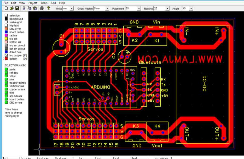
Gerber files use ASCII text to provide instructions for positioning “flashes” (shapes) to construct images corresponding to each layer of a PCB design. There are a few key elements:
- Apertures – Geometric shapes like circles or polygons that define flash outlines.
- Flashes – Instances of an aperture used to make marks or draw image outlines.
- Coordinates – X/Y coordinate positions locating where flashes are placed.
- Operations:
- Interpolation – Moving between coordinates with straight/curved lines.
- Region fill – Filling a closed shape with flashes.
- Aperture changes – Selecting different aperture shapes.
By combining these primitives, detailed PCB layer images can be constructed from bare copper to solder mask.
Gerber File Extensions
Standard Gerber files use the .gbr extension. Some other file extensions seen:
- .gtl – Gerber template file with aperture definitions.
- .gbo – Gerber board outline layer.
- .gbs – Gerber soldermask layer.
- .gbl – Gerber copper layers.
- .gm1 – Gerber top copper layer.
- .gm13 – Gerber bottom copper layer.
There are also numbered extensions for inner copper layers (gm2, gm3, etc.) By convention, layer numbers increase from top to bottom.
Why Use Gerber Files for PCBs?
There are several advantages provided by the Gerber format:
- Neutral File Exchange – Gerber is not tied to any specific CAD tool, allowing easy transfer between different PCB software packages.
- Standardization – Gerber provides consistency across the entire PCB industry. Fabricators accept Gerbers from all designers.
- Separate Layer Images – Splits PCB layout into individual layer images needed for photolithographic fabrication.
- Wide Support – Accepted by all PCB fabrication equipment, software, and processes.
- Compact Format – Files are relatively small and easy to transfer.
- Longevity – Gerber has been used for decades and continues to be updated. Format will be around indefinitely.
Overall, Gerber delivers a standardized and widely adopted format for taking PCB designs through manufacturing.
Gerber File Creation in PCB CAD Software
Specialized PCB layout software is used to design boards and output production-ready Gerber files. Common options:
Altium Designer
- Industry leading PCB tool used across many companies.
- Built-in Gerber file generation with extensive layer control.
- Jobs panel automates file output with layer visibility settings.
KiCad
- Open source, freely available PCB design suite.
- Plotting tool outputs customizable Gerbers directly from the GUI.
- Excellent community support for KiCad Gerber creation.
Eagle
- Long running, popular hobbyist PCB CAD.
- CAM Editor provides easy point and click Gerber file generation.
- Limited layers may require workarounds for full manufacturing output.
- Autodesk now owns and integrates with Fusion 360.
FreeCAD
- Open source 3D modeling tool with PCB workbench for DIY boards.
- TechDraw workbench can output 2D manufacturing files.
- Extra configuration required compared to dedicated PCB software.
And many more! Every PCB design system can ultimately output Gerber files required for board fabrication.
Typical PCB Gerber Layers
A complete set of Gerber files provides each layer needed to make a finished PCB. Here are some typical layers:
Copper Layers
- Top Copper (GTL/GM1) – Copper traces on top surface.
- Bottom Copper (GBL/GM13) – Copper traces on bottom surface.
- Inner Copper Layers (GM2, GM3, etc.) – Copper traces on layers between surfaces.
Solder Layers
- Top Solder Mask – Solder resist layer covering top copper.
- Bottom Solder Mask
- Top Solder Paste – Screen printed solder on top surface.
- Bottom Solder Paste
Overlay Layers
- Silkscreen – Printed component outlines, logos, text.
- Drill Drawing – Locations of drill holes needed.
Profile Layer
- Board Outline – Shape of finished PCB.
Miscellaneous
- Copper Thieving – Copper shapes for better plating.
- Cutouts – Pocket milling extents.
- Arc layers – Non plated holes.
Gerber File Order and Layer Stacking
The order of Gerber files determines the layer stackup during PCB manufacturing. Files must be provided in a logical sequence:
- Copper Layers – Lowest numbers on bottom. Usually Bottom, then Inners, then Top.
- Solder Layers – Bottom layers first. Solder Paste then Solder Mask.
- Overlays – silkscreen first, then drills/holes.
- Board Profile – Outline last.
Following this standardized order ensures Gerbers align across the stack as intended. The PCB fabricator may request a particular sequence.
Why So Many Gerber Files?
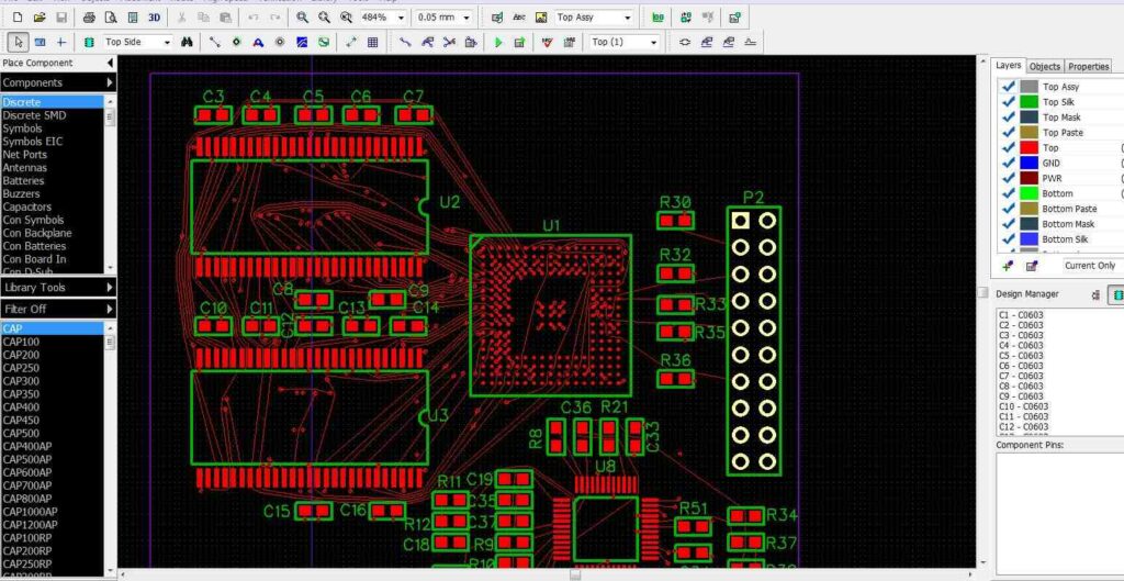
A PCB design can require over a dozen different Gerber files. Why so many?
- Photoplotting – Each layer is a separate physical photomask. Output as an individual file.
- Front-to-back alignment – Must distinguish layers on top vs bottom of board.
- Inner layers – Complex boards have traces on internal layers requiring individual Gerbers.
- Separate processing – Different fabrication steps for solder mask, silkscreen, copper etching, etc.
- Flexibility – Allows customization of file outputs. Include only needed layers.
Multiple Gerber files provide full control over each PCB layer during fabrication.
How to Generate Gerber Files
The basic process for creating manufacturable Gerber files from a PCB CAD tool:
- Set Layer Colors – Give each layer a unique color for visibility.
- Enable Layers – Turn on visibility of all layers needed for fabrication.
- Adjust Settings – Set proper apertures, D codes, polarity, etc.
- Load Fabrication Outputs – Select profile with all necessary layer types.
- Generate Files – Save individual Gerber files for each enabled layer.
- Verify – Do a test plot check before sending to PCB manufacturer.
Following the vendor’s specifications for settings produces fabrication-ready Gerbers.
Gerber File Errors to Avoid
Some common mistakes that can render Gerber files unsuitable for PCB production:
- Missing key layers for circuit fabrication.
- Extraneous layers not used in PCB process. Wastes effort.
- Wrong file order for layer stackup. Can cause misalignment.
- Incorrect apertures or D codes for manufacturing process.
- Polarity (dark vs clear) flipped on layers. Trace images will be wrong.
- Layer alignment offsets. Layers not stacked properly.
- Duplicate layers instead of proper top/bottom designation.
- Plans for scoring/milling not indicated in file outputs.
Careful checking of the Gerber sequence prevents errors and delays in PCB production.
Validating Gerbers with CAM Plots
CAM (computer-aided manufacturing) plots from the PCB software are essential for verifying Gerber files before sending to fabrication:
- Composite – Shows all layers together, confirming alignment.
- Individual – Spot check each layer for proper content.
- Top-bottom mirrors – Catch polarity flips between top and bottom.
- Full-scale – Actual 1:1 print scale, not shrunk down.
- All drill holes – Verify with pin/via drill drawing layer.
Thoroughly inspecting CAM plots lets you fix any Gerber issues early and avoid problems during manufacturing.
Sending Gerber Files to PCB Fabrication
Once Gerber files are validated, upload the set to your PCB manufacturer:
- Zip archive – Keep all files together in one .zip file.
- README – Include a text file with notes.
- Layer documentation – List of all included layers and purpose.
- Order notes – Any special instructions on layer stackup or settings.
- Contact info – Your name and contact details.
- ** Fab specs** – Note board size, layer count, thickness, etc.
- Fabricator checklist – Review to catch missing files, improper settings.
Good documentation ensures your Gerbers are quickly processed and sent to manufacturing without issues.
Gerber File Generation Checklist
Here is a helpful checklist when exporting Gerber files for fabrication:
- All necessary fabrication layers enabled
- Layer order and polarities set correctly
- Appropriate file extensions used for each layer
- Layer alignment offsets checked
- Apertures, D codes set for manufacturing
- No duplicate or extraneous layers
- CAM plots verified for each layer
- README and docs included
- Zip archive sent to PCB manufacturer
Following this standardized checklist helps avoid common Gerber file issues that can delay your PCB build.
Gerber File Viewers
While CAM plots primarily validate Gerbers, you can also visually inspect files with free Gerber viewers:
- Gerbv – Open source Gerber viewer for Linux. Very customizable.
- ViewMate – Freeware Gerber viewer for Windows. Easy and intuitive.
- Kicad StepUp – Built in viewer for KiCad. Light on features.
- Online Viewers – PCB fabrication shops offer online file viewers.
Useful for quickly eyeballing individual layers when checking Gerber files.
The Future of Gerber Files
Gerber format has been the standard for PCB fabrication data for decades. Looking ahead:
- Here to stay – Gerber is entrenched in PCB processes and will remain the norm.
- Updates – The format continues to be updated to support new features.
- More verification – Expect more validation tools to catch Gerber errors pre-manufacturing.
- Direct drive – Some very advanced equipment may move away from Gerber photoplots, but will still accept Gerbers.
- Non-PCB uses – Gerber is being used for printing trace patterns in conductive inks, ceramics, and textiles.
While it originated in 1970s photoplotting, the versatility and ubiquity of the Gerber format ensures it will remain vital for PCB design and fabrication for the foreseeable future.
Frequently Asked Questions
What is the difference between Gerber and drill files?
Gerber files define the copper layers, solder mask, silkscreen graphics, and board profile. Drill files specify the locations, sizes, and properties of holes to be drilled in the PCB. Both are required together for fabrication.
Can I open Gerber files in PDF format?
No, Gerber files use a specialized ASCII format to encode photoplotting image data. They cannot be natively opened in PDF viewers or other image editors. Some Gerber viewers can export a visual representation to PDF.
Do I need to zip Gerber files before sending to fabrication?
Zipping the Gerber files into a single archive (.zip) is recommended. This keeps all files together in one package for easier transfer and avoids any issues with certain OS environments stripping file extensions.
What is the most common Gerber file error made by new PCB designers?
The most common mistake is forgetting to enable the right set of layers before generating Gerber files. This can lead to missing critical layers like copper or solder mask. Carefully checking that all needed layers are visible avoids this issue.
Can I use Gerber files for submitting PCB designs to assembly services?
No, assembly services need a different file format such as IPC-2581 that includes PCB fabrication data plus information on components, placement, and the bill of materials. Gerber files define the bare board itself but lack assembly-related data.

