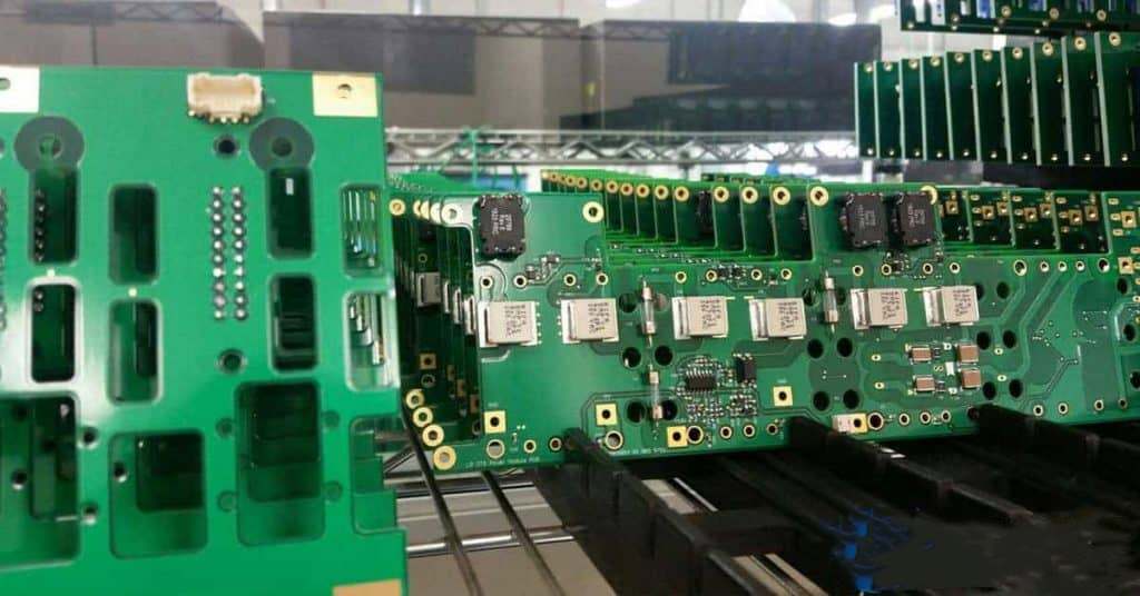
Printed circuit board (PCB) assembly involves soldering various electrical and electronic components like resistors, capacitors, ICs, connectors etc. onto a PCB to create a fully functional electronic circuit. Turnkey PCB assembly refers to outsourcing the entire assembly process to a specialized PCB assembly service provider.
The assembly partner takes responsibility for procuring all the required components, loading them onto the PCB, soldering, cleaning, inspecting and testing the boards, and delivering fully assembled PCBs ready to be integrated into electronic products. This article provides a detailed overview of what turnkey PCB assembly involves, its benefits, key steps in the process, factors to consider when choosing an assembly partner, and more.
What is Turnkey PCB Assembly?
Turnkey PCB assembly refers to contracting a PCB manufacturing and assembly company to assemble printed circuit boards completely from start to finish as per the client’s product specifications. It is also referred to as full-turnkey assembly.
In this approach, the OEM (Original Equipment Manufacturer) designing the electronic product would provide the PCB fabrication files (gerbers, schematics, BOM or bill of materials, assembly drawings etc.) to the turnkey vendor.
The vendor is then responsible for:
- Fabricating the bare PCBs as per the supplied fabrication data files
- Procuring all the required components listed in the BOM
- Loading (placing) the components onto the fabricated PCBs
- Soldering the components using SMT (Surface Mount Technology) and/or through-hole techniques
- Performing post-soldering processing like cleaning and coating
- Testing the assembled PCBs for defects using AOI (Automated Optical Inspection)
- Performing functional testing if required based on provided test specifications
- Shipping fully assembled and tested PCBs to the OEM
By outsourcing these processes, the OEM does not need to purchase SMT equipment, maintain inventory, staff assembly lines etc. This allows them to focus on their core competence – designing the product hardware and firmware. Turnkey assembly provides a faster, more cost effective solution vs. in-house assembly for low and medium volume production.
Benefits of Turnkey PCB Assembly
Choosing turnkey assembly over in-house assembly provides several important benefits:
Faster Time-to-Market
- Eliminates need for OEM to purchase assembly tools, set up lines and train operators. Products reach market faster.
Cost Savings
- No capital expenditure on assembly tools and inventory. Economies of scale bring significant per unit cost reduction.
Improved Quality
- Mature processes, specialized tools, trained staff and testing lead to higher assembly quality and yield.
Flexibility
- Easy scale up/down based on demand. No overhead of maintaining under-utilized equipment or staff.
Focus on Core Strength
- OEMs can focus on design and innovation rather than manufacturing logistics.
Simplified Logistics
- Single point of contact for PCB fabrication through assembly. Reduction in OEM overheads.
Access to Advanced Technology
- Latest high speed surface mount equipment, soldering techniques and inspection systems.
Risk Mitigation
- Turnkey vendor is responsible for assembly process performance and issues. OEM bears lower risk.
Real-time Visibility
- Options like webcam monitoring and automated data logs provide excellent process visibility.
For low to medium volume production runs, turnkey PCB assembly clearly provides tremendous benefits over in-house assembly. However, for very high volumes, OEMs may still consider investing in their own assembly lines.
Turnkey PCB Assembly Process Steps
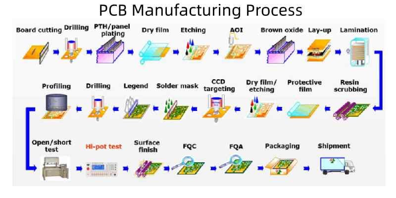
The major stages involved in turnkey printed circuit board assembly are:
1. Design and Fabrication Data Preparation
- OEM creates PCB layout, schematics, BoM (bill of materials), assembly and fabrication drawings.
- Gerber files, centroid data, pick-and-place (XYRS) files, assembly instructions etc. are provided to assembly vendor.
2. PCB Fabrication
- Vendor fabricates bare PCBs using supplied fabrication data such as gerber files.
- Common processes like imaging, etching, hole drilling, plating, routing and testing are done.
3. Component Procurement
- Vendor does bill of materials analysis and procures all parts – both SMT and through-hole components.
- Preferred component packaging styles and quantities are considered.
4. Solder Paste Stencil Creation
- Laser-cut solder paste stencils are fabricated based on PCB design data.
- Used for applying solder paste accurately on SMT pads during pick-and-place stage.
5. Surface Mount Device (SMD) Placement
- SMT components are precisely placed on target PCB pads using automated pick-and-place machines.
- Advanced optical alignment systems ensure accuracy down to 0.01mm.
6. Solder Paste Reflow
- PCBs with SMT components are passed through IR/convection reflow ovens.
- Solder paste is heated to liquid state, forming reliable mechanical and electrical joints.
7. Through-Hole (THT) Component Insertion
- Components with wire leads like connectors are inserted into plated through-holes.
- Done manually or using automated insertion equipment.
8. Wave Soldering
- PCB underside is passed over molten solder wave to solder through-hole leads.
- Provides very rapid, reliable soldering of high lead count components.
9. Post Solder Processing
- Flux residues cleaned using water, solvents or saponification.
- Boards are dried, and conformal coating applied if specified.
10. Automated Optical Inspection
- Assembled PCBs are inspected using 2D and 3D AOI systems.
- Checks for missing, misaligned or defective components, solder defects, bridging etc.
11. Functional Testing
- Based on test specifications, electrical tests validate functionality.
- Continuity checks, Boundary Scan, Flying Probe and ICT testing done.
12. Conformal Coating
- Protective plastic coatings applied manually or using selective spraying.
- Improves reliability against moisture, vibration, abrasion etc.
13. Programming
- For PCBAs with MCUs or FPGA, firmware is loaded into memory using programmers.
14. Final Integration
- Accessories like connectors, hardware, labels, cables are added to produce finished PCB assembly.
15. Packaging and Shipping
- Assembled PCBs are packaged with ESD protection.
- Shipped to OEM facility using appropriate transport mode.
This end-to-end turnkey approach minimizes the effort required from the OEM while ensuring a high-quality assembly process using industry-proven techniques.
Factors to Consider when Selecting a Turnkey Assembly Partner
Choosing the right turnkey PCB assembly partner is crucial for getting high quality finished boards delivered on time. Here are some key factors to evaluate:
Technical Capabilities
- Range of PCB types that can be assembled – multilayer, HDI, flex-rigid etc.
- SMT equipment sophistication – high speed, high accuracy, advanced capabilities
- Types of component packaging that can be handled – 0201 chips, BGAs, connectors etc.
- Experience with dense PCB assemblies and fine feature sizes
Quality Systems
- Compliance certification – ISO, IPC, ITAR etc.
- Process controls and inspection systems used
- Qualifications and training of assembly technicians
- Quality metrics like defect rates, yields etc.
Assembly Volumes
- Ability to scale up or down flexibly based on production needs
- Infrastructure capacity – cleanrooms, SMT lines, test stations etc.
Supply Chain Capability
- Procurement of long-lead, obsolete or hard-to-find components
- Vendor managed inventory and JIT delivery
Program Management
- Account management and engineering support
- Manufacturing planning, scheduling and order tracking systems
Continuous Improvement
- Engineering collaboration for design-for-manufacturing
- Process enhancement using statistical methods like Six Sigma
Cost
- Pricing model – per unit, volume based etc.
- Value-added services included
- Payment terms
Logistics
- Handling of international shipments
- Customs coordination expertise
- Shipping locations to provide regional support
Eco-system
- In-house vs. outsourced manufacturing resources
- Partnerships with suppliers, test labs etc.
By thoroughly evaluating turnkey assembly partners on these aspects, OEMs can select the right strategic provider for their specific PCB assembly needs. This helps maximize quality, reliability, cost control and on-time delivery.
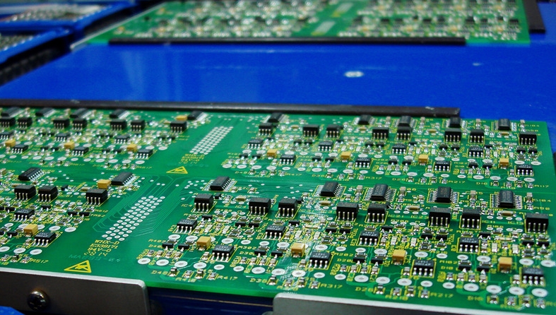
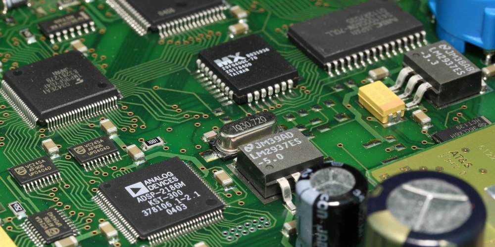
SMT Assembly Process In-Depth
SMT or surface mount technology refers to the process of mounting electronic components directly onto the surface of a PCB without through-hole leads. It enables automated high-speed component placement and miniature electronics assembly. Here is a closer look at the key stages:
Solder Paste Stencil Creation
The solder paste stencil is a thin metal sheet that is laser cut with apertures matching the PCB land patterns. It is aligned over the PCB and solder paste is spread over the stencil. The paste squeezes through the apertures, depositing precise volumes onto the SMT pads. Laser cutting and electroformed nickel stencils allow fine feature printing down to 0.15mm pitch components.
Laser-cut solder paste stencil
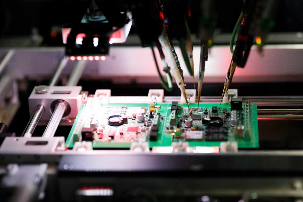
###High Speed Pick-and-Place
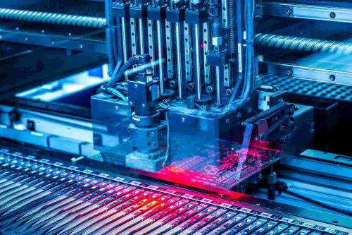
SMT components are supplied in reels, trays or sticks which are loaded onto automated pick-and-place machines. Feeders bring the parts to pickup locations inside the machines. Camera and laser guided robots pick components and place them precisely onto the solder paste-coated PCB pads.
Modern pick-and-place systems like quad-gantry Yamaha YV40X can achieve speeds exceeding 100,000 chip placements per hour (CPH) with accuracy of 0.01mm for microchips down to 0201 (0.6mm x 0.3mm) size.
High speed quad-gantry pick-and-place system
Solder Paste Reflow Process
After placement, PCB assemblies pass through reflow ovens where multiple heating zones raise the temperature to melt the solder paste and “reflow” it into solder joints. These zones – preheat, soak, reflow, cool-down – follow programmed thermal profiles to control soldering quality.
Typical solder reflow oven with multiple heating zones
Reflow can use convection heating, IR radiation, laser soldering and even localized microwaves. The peak temperature is around 240°C to 260°C depending on the solder composition used. Nitrogen blanketing prevents oxidation. The liquid solder wets the metal surfaces and solidifies into reliable solder joints as temperature drops.
Cleaning and Coating
Any post-solder flux residues are cleaned off using water, alcohol, or solvents in spray-in-air inline systems. Detergent solutions can also used for saponification cleaning. PCBs are then dried, and conformal coatings like acrylic, silicone, urethane or parylene can be selectively applied to enhance reliability against dust, moisture and other contaminants.
Automated Inspection
After reflow, boards move to automated optical inspection (AOI) stations where 2D and 3D image sensors along with software analyze each assembly in detail looking for defects like missing parts, tombstoning, misalignments, solder bridging etc. Powerful algorithms can inspect thousands of joints per board at high speeds, far surpassing manual visual inspection.
Touch-up and Re-work
If any defects are identified, manual touch-up using soldering irons and hot air can be done. Inspection helps improve processes by pinpointing problem areas. For defective components not repairable on-line, boards move to dedicated re-work benches for removal and replacement of specific parts. This allows recovery of valuable PCB assemblies.
Final Functional Test
After inspection, each populated PCB undergoes electrical testing either off-line using fixtures or in-circuit using test probes/pogo pins. Continuity checks validate connections while functional tests verify the board operates as per specifications. This screen out any latent or “infant mortality” defects. Flying probe testers and boundary scan are commonly employed.
This sequence of SMT assembly processes allows rapid population of PCBs with a wide variety of surface mount components while assuring quality standards.
Through Hole Assembly Process
While SMT is best suited for mounting small components, many boards also use larger leaded components like connectors, relays, transformers etc. which cannot be surface mounted. These through-hole components are assembled as follows:
1. Component Insertion
Components with axial or radial leads are inserted manually or using automated insertion machines into plated through holes. Machines allow rapid insertion of multiple components in a single stroke.
2. Clinching and Cutting
The leads may be clinched using anvil type tools to provide preliminary retention. Excess lead length is trimmed using cutting blades or shearing tools.
**3. Wave Soldering **
The assembled board underside is passed over a flowing wave or jet of molten solder at 230-270°C. The solder wets and adheres to exposed pad areas and component leads.
4. Cleaning
Excess flux is cleaned off using solvents, water or saponification. This prevents residue buildup.
5. Inspection
Boards are visually inspected under magnification or X-ray imaging to check for shorts, opens and good fillet formation.
6. Re-work
If needed, manual re-work using soldering irons is done to correct any joint defects found during inspection.
Wave soldering provides very high throughput for boards with high through-hole component counts. For boards with fewer through-hole parts, manual soldering may be used.
Failure Analysis in PCB Assembly
Despite stringent process controls, some small percentage of defects and failures still occur during PCB assembly. When this happens, failure analysis (FA) is performed to determine the exact physical and electrical root cause so that corrective actions can be taken. Some key failure analysis techniques are:
Visual Inspection
- Detailed visual examination under stereo microscope helps identify external defects.
X-Ray Imaging
- X-ray radiography reveals internal features and defects not visible externally.
Thermal Profiling
- Monitoring temperatures at key points can identify defects in the thermal process.
Cross-Sectioning
- Cutting through suspect joints and examining under microscope shows internal flaws.
Electrical Testing
- In-circuit tests, function tests and flying probes verify electrical faults.
SIMS Analysis
- Secondary ion mass spectrometry analyzes chemical composition and contamination.
SEM/EDS Analysis
- Scanning electron microscope combined with energy-dispersive X-ray spectroscopy determines structure and elemental composition.
Focused Ion Beam
- FIB cross-sectioning and imaging shows detailed internal features.
Infrared Imaging
- IR thermography maps thermal characteristics and hot spots.
3D X-ray CT
- 3D X-ray computed tomography gives detailed defect localization in three dimensions.
PCB failure analysis employs a combination of these tools to pinpoint the source of assembly defects so that process steps can be corrected.
Key Factors for Quality Assembly
To achieve reliable, high-yield PCB assembly, several factors have to be well controlled:
- Design for Manufacturing (DFM) – PCB layout itself should consider assembly factors like component spacing, trace geometries etc.
- Process Capability – Assembly equipment such as pick-and-place and reflow ovens must have precision and repeatability.
- Controlled Processes – Standard operating procedures for each step ensures consistency.
- Skilled Technicians – Operator training and certification is vital for inspection, touch up and handling.
- Component Management – Use of properly packaged, ESD-safe parts and FIFO stock rotation.
- Contamination Control – Cleanroom assembly and handling protocols minimize defects.
- Solderability – Parameters like temperature profiles, paste volumes, stencil condition directly affect solder joint formation.
- Test Coverage – Thorough testing and failure analysis drives yields up.
With close attention to these factors, turnkey assembly services are able to deliver defect rates of less than 100 ppm (parts per million) on even complex, dense boards. The more critical a product is, the more stringent assembly controls become. Medical, defense and aerospace PCBs demand the highest quality levels.


