A solder paste stencil is a key consumable used in printed circuit board assembly for applying precise and uniform solder paste deposits onto pads prior to surface mount component placement.
This article provides an extensive overview covering stencil types, manufacturing methods, working principles, key functionalities, parameters and performance factors involved in solder paste stencil operations.
Why Use a Solder Paste Stencil?
In a PCB assembly process workflow, a solder paste stencil serves the critical step of programmatically transferring solder paste from carrier to pads for holding components before soldering. This fulfills several objectives:
Consistent Deposit Patterns
Stencils contain cutouts as per PCB land patterns allowing replicable, mistake-proof printing of small solder paste dots/bricks on many boards.
Selective Application Control
Unlike other methods like dispensing, dipping or spraying, stencils localize application only to required pads areas through openings.
Precision Dosing
Deposit volumes are precisely defined by stencil thickness, alloy viscosity and aperture designs enabling very low variation.
Process Compatibility
Stencil operation integrates smoothly within automated board stuffing lines using standard material formats.
Thus, paste stencils crucially enable accurate, repeatable paste transfer at scale in SMT lines.
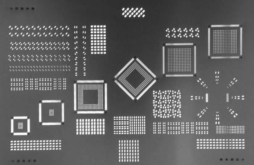
Types of Solder Paste Stencils
Stencils are divided into categories based on manufacturing approach and degree of durability/longevity.
Laser-Cut Steel Stencils
Thin stainless steel sheets are engraved by laser systems to ablate openings constituting industry workhorse for premium accuracy and resilience. Reusable over thousands of prints.
Electroformed Nickel Stencils
Build 3D metal aperture profiles galvanically with accurate dimensional control. Extensive longevity due to robustness but high startup cost.
Laser-Cut Polyimide
Non-conductive Polyimide film media directly lasered to create openings. Avoid paste clogging issues and suitable for controlled impedance PCBs. Disposable.
Based on trade-offs like accuracy, initial tooling expenses versus reuse potential and design complexity – appropriate stencil technology gets selected for a PCB program.
Working Mechanism of Solder Paste Stencil
The core operational principles underlying stencil-mediated solder paste application involves:
Step 1: Solder paste containing metal alloy suspended uniformly in flux vehicle is applied over stencil surface forming a roll/bead.
Step 2: A squeegee blade traverses under specific pressure and angles pushing the paste into stencil apertures completely filling them.
Step 3: The stencil is carefully lifted vertically off the PCB to release precise paste deposits imprinted onto pads mirroring land patterns.
Step 4: Component placement occurs over pads with paste transferring onto leads forming both electrical and mechanical attachment.
Step 5: Reflow process melts the paste deposit transforming it into an intermetallic solder joint through alloy reflow and flux cleansing action.
Key Aspects Governed by Solder Paste Stencils
Certain vital assembly process characteristics hinge greatly on parameters built into the stencil design itself:
Printing Accuracy
Aperture positioning precision coupled with stencil-to-board alignment controls pattern transfer fidelity without shifts.
Deposit Volumes
Aperture sizes, web thickness, area ratios determine the print paste volumes per pad helping meet solder joint quantity needs.
Process Windows
Aspects like print speeds, separation gaps, stencil life etc. get dictated by stencil properties guiding equipment settings.
Bridging Risks
Aperture spacing/size ratios considering alloy suspension particle sizes require sufficient guardbanding to avoid adjacent print merging.
Solder Balling
Aperture land coverage percentages coupled with termination geometries guide ball grid array (BGA) paste release properties after reflow.
Thus stencil design aspects directly impact process robustness and assembly quality necessitating their careful optimization.
Key Parameters in Solder Paste Stencils

Several user-specifiable stencil parameters need appropriate selection based on product profiles to achieve viable process performance:
Thickness/Height
Typically laser cut steel stencils range from 100 to 150 μm while thicker nickel stencils span 200 to 250 μm. Impacts paste release.
Aperture Shapes/Dimension
Land pattern, registration needs and alloy particle sizes guide aperture dimensions. Round vs squared openings offer different separation.
Stencil Perforation Density
Total aperture area percentage relative to stencil area indicating paste transfer loads in print stroke demanding appropriate frame/foil thickness support.
Foil Tensioning
Nickel tensioning levels or steel frame styles control foil rigidity/planarity during printing avoiding separation gaps from PCB pads.
Underside Etching Profiles
Underside cavity shapes with tapered, cylindrical or rectangular cross-sections provide fine-tuning of paste release dynamics especially for microdeposit control.
Careful selection of stencil attributes tailored to product needs ensures achieving solid printing yield with no bridging faults or Skipping.
Laser-Cut VS Electroformed Stencil Comparison
Performance Comparison
| Parameter | Laser-Cut Steel | Electroformed Nickel |
|---|---|---|
| Accuracy | +/- 5 mil | +/- 2 mil |
| Aspect Ratio | 1:10 | >1:10 |
| Aperture Density | Standard | Very High |
| Stencil Life | < 5000 prints | > 50000 prints |
| Bridging Resistance | Moderate | Maximum |
| Print Definition | Nominal | Excellent |
| Initial Tooling Time | Fast | Slow |
Electroforming surpasses laser patterning in reliability metrics critical for fine pitch components but lags on cost and lead times suiting high volume applications.
Solder Paste Printing Process Steps
The sequence of stencil printing operations across SMT assembly consists of:
1. Stencil Mounting
Secure stencil foil in assembly tool aligning mounting fiducials for accuracy.
2. Print Setup
Define squeegee type, angle, paste type, speed, separation and stroke settings.
3. PCB Loading
Machine vision aligns PCB to stencil reference fiducials.
4. Print Stroke Squeegee spreads paste forcing into apertures completely filling them.
5. Stencil Separating At optimized peel off rates, stencil detaches from PCB cleanly leaving precise paste dots.
6. PCB Unloading Prints get inspected before unloading. Stencil undergoes periodic underwipe cleaning.
Solder Paste Printing Defect Modes

Despite well-designed stencils, defects in prints can manifest due to processing factors:
Bridging Paste coalescence across adjacent pads caused by insufficient web spacing, particle overflow or alignment deviations.
Insufficient Transfer Efficiency Incomplete paste release volumes indications nozzle clogging or inadequate fill during squeegee pass.
Skips/Missing Deposits Pads fully devoid of prints owing to stencil-PCB separation gaps, poor aperture cleaning or uneven foil tensions.
Smearing Paste residue laterally spread on PCB surface because of excessive PRINT stroke separation speeds.
Thixotropic Recovery Issues Poor paste viscosity recoveries after printing when left idle for long durations leads to inadequate volumes and shapes.
Through put-up print monitoring, root causes behind defects get diagnosed and corrected via stencil/machine adjustments preventing downstream soldering issues.
FAQs
Can solder paste be reused?
Multiple print stroking runs using the same paste are not recommended since already-loaded paste loses viscosity uniformity with metal particles settling over time degrading transfer efficiency in subsequent prints. Fresh paste works best.
What materials are used for stencils?
Stainless steel grades like SS-304/305 with 150/100 μm are prevalent while nickel/molybdenum alloys span larger thickness range owing to close CTE match with PCBs providing dimensional stability.
How does one clean underneath stencil apertures?
Periodic undersideCLEANINGHELPSeffective debris removal preventing clogging using wiping medications and nanocoated polyurethane squeegees while maintaining foil texture. Stencil wash systems provide automated cleaning.
Can solder paste be stored at room temperature?
Paste is stored frozen typically since properties like viscosity, tackiness and flux activity get impacted severely by thermal exposure. Refrigerated storage at 2-10°C also works temporarily but best practice is minimizing paste thaw-refreeze frequency.
How does one dispose of solder paste?
Unused solder paste containing metals, solvents/resins and activators requires special disposal procedures meeting regional safety and environmental regulations. Tin-lead solders mandate stricter controls given toxicity concerns.
Thus, optimal stencil usage forms a vital, versatile bridge between PCB fabrication and component mounting ultimately realizing quality solder interconnects through precision paste transfer.


