Introduction
Soldering is the process of joining electronic components to printed circuit boards (PCB) using melted solder metal alloys. It is an essential step in assembling electronic devices and circuits. There are various techniques, types and materials involved in soldering PCB assemblies reliably and effectively.
This comprehensive guide covers all key aspects of PCB soldering. It explores the most common soldering methods, types of solder joints, solder compositions, flux usage and the overall soldering process flow. With the right techniques and materials, high-quality solder joints can be achieved.
PCB Soldering Techniques
There are several techniques used for soldering components to PCBs in electronics assembly. The main soldering methods include:
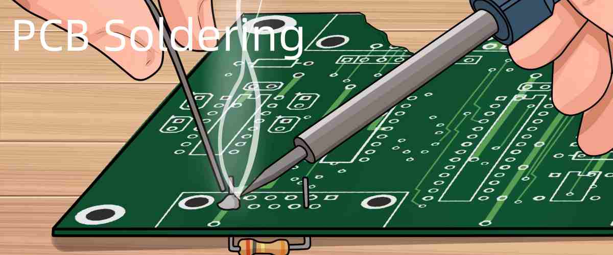
Hand Soldering
Hand soldering is done manually using a soldering iron. It involves:
- Applying solder wire to joints
- Heating pads and leads to melt solder
- Allows small-scale rework and repairs
Hand soldering may be suitable for assembling prototypes or small production runs. But it does not scale well for volume manufacturing.
Reflow Soldering
Reflow soldering is the automated process of soldering surface mount devices (SMD) using solder paste and a reflow oven. Steps include:
- Solder paste is printed on PCB pads
- Components placed on paste deposits
- Board passed through convection reflow oven
- Oven heat melts solder paste to form joints
Reflow soldering is used for almost all high-volume PCB assembly with SMD components.
Wave Soldering
Wave soldering machines solder through-hole component leads by passing the PCB over a molten wave of solder. The process involves:
- Flux applied to remove oxidization
- Bottom side pre-heated
- PCB contacted with solder wave
- Solder wets leads and forms joints
- Excess solder removed
Wave soldering provides fast automated soldering of through-hole components.
Selective Soldering
Selective soldering uses a specialized soldering head to target individual joints. Parameters are:
- Programmed into machine
- Miniature solder nozzle
- Bottom-side heater
- Used for repairs or partial rework
Selective soldering provides more flexibility than wave soldering for small production runs.
Types of PCB Solder Joints
There are several types of solder joints used to affix components to PCBs:
Through-Hole Joints
Through-hole joint have leads inserted through holes in the PCB and soldered on the opposite side:
- Allows mechanical anchoring
- Double-sided anchoring provides strength
- Best for high-vibration environments
- Not suitable for dense, compact PCBs
Surface Mount Joints
Surface mount (SMD) joints connect components directly to the surface pads of the PCB without leads passing through holes. Advantages include:
- Allows greater component density
- Automated assembly
- Smaller pads and pitches
- Faster production
- Suitable for complex, compact PCBs
Press-Fit Joints
Press-fit PCB assembly presses component pins into plated through-holes. Benefits are:
- No soldering required
- Easy component replacement
- Withstands high temperatures
However, press-fit joints have lower strength than soldered joints. They are only used for connectors or in specialized applications.
Solder Compositions
PCB solder is made from metallic alloys that melt at relatively low temperatures for joining. Common solder compositions include:
| Composition | Melting Point | Properties | Use Cases |
|---|---|---|---|
| 60/40 Sn/Pb | 183°C | Good flow, low cost | General purpose (being phased out due to toxicity) |
| 63/37 Sn/Pb | 183°C | Improved properties | Aerospace/military applications where lead is still permitted |
| SAC 305 | 217°C | Lead-free, good wetting | Most common lead-free solder |
| SAC 105 | 217°C | Thinner joints | Fine pitch components |
| SAC 405 | 225°C | Higher strength | Harsh environment electronics |
| Silver | 960°C | High strength, conductivity | Power electronics, RF applications |
Many alloy compositions are available to suit different soldering requirements. Lead-free solders like SAC alloys have become predominant to meet environmental directives.
Solder Flux Types
Flux is applied during soldering to:
- Remove surface oxides
- Improve solder wetting
- Prevent re-oxidation
Common solder fluxes include:
| Type | Properties | Applications |
|---|---|---|
| Rosin (RA/RMA) | Weak activity, non-conductive residue | Common in electronics assembly |
| Water-soluble | More active, residue can be washed | Consumer electronics |
| No-clean (NC) | Moderate activity, leaves residue | Automated soldering where cleaning not practical |
| Organic | Aggressive organic acids | Difficult metals like aluminum |
Selecting the right flux for a particular soldering application involves tradeoffs between activity and residue effects.
Soldering Process Step-By-Step

The electronics assembly soldering process generally follows these steps:
- PCB Fabrication – Bare PCBs are fabricated with pads and plating.
- Stencil/Screen Printing – Solder paste applied to pads on SMD PCBs.
- Component Placement – Components placed on prepared boards.
- Reflow – For SMD parts, board passes through conveyor reflow oven.
- Wave/Selective Soldering – For through-hole parts, wave or selective soldering is used.
- Cleaning – Flux residues cleaned depending on flux type used.
- Inspection – Solder joints checked for defects with AOI.
- Conformal Coating – Protective coating applied for environmental resistance.
- Testing – Boards electrically tested and debugged if needed.
- Final Assembly – Any additional mechanical assembly performed.
The soldering steps provide both mechanical and electrical connections between components mounted on the PCBs. This assemble electronic circuits ready for integration into finished products.
Soldering Process Parameters
Achieving high-quality soldering depends on optimizing these key process parameters:
The solder bath or iron tip must attain a temperature high enough to fully melt the solder alloy used. Excess temperature risks damage.
Dwell Time
The contact duration between the joint and heat source must be sufficient to form the intermetallic bond.
Heating Ramp Rate
The rate of heating during reflow should follow recommended thermal profiles based on the solder alloy. Too fast risks cracks.
Cooling Rate
How quickly solder joints cool after reflow or wave soldering affects crystal structure. Slow cooling with low temperature gradients is best.
Flux Activity and Residue
The flux must be active enough to remove surface oxides but not overly aggressive to eat away at the joint over time. Minimal residue left behind is ideal.
Solder Volume and Fillet Shape
The optimal shape and amount of solder should wet the joint completely without excessive bulk or creating shorts.
Soldering Defects
Common soldering defects include:
- Cold joints – Incomplete wetting due to low heat
- Cracks – Caused by flexing of brittle joints
- Voids/porosity – Trapped gases weaken joint
- Bridging – Solder spans between joints causing short
- Icicles/spikes – Flux residue appears like icicles
- Dewetting – Joint pulls back from pad due to contamination
- Insufficient wetting – Pad not fully covered by solder
Thorough inspection of solder joints is needed to detect defects and implement corrective actions for consistent soldering quality.
Improving Solder Joint Reliability
Reliable solder joints withstand mechanical stresses, thermal cycling, vibration and other rigors over the life of electronic devices. Methods to enhance reliability:
- Matching component footprint, pad and land pattern geometries
- Applying sufficient solder paste for good wetting
- Following proper reflow thermal profiles
- Allowing sufficient cooling time to form uniform crystals
- Minimizing flux residues and ionic contamination
- Conformal coating to retard environmental damage
- Reducing board flexing through mechanical design
High-reliability soldering requires attention to material selection, process parameters, inspection rigor and conformal coating.
Latest Trends in PCB Soldering
Some recent developments impacting PCB soldering include:
- Lead-free solders – Regulatory and environmental pressures continue promoting lead-free alloys.
- Alloy optimization – Solder metallurgies fine-tuned for thermal cycling reliability.
- Miniaturization – Microjoints, thin boards, HDI, and tighter tolerances presenting challenges.
- Automation – AI-assisted optimization of soldering parameters.
- In-process inspection – Automated optical inspection immediately after soldering.
- Non-solder interconnects – Emerging alternatives like conductive adhesives for niche applications.
Even after decades of innovations, there are still active efforts to enhance PCB soldering processes and materials.
Conclusion
In electronics manufacturing, PCB soldering provides both electrical conduction and mechanical adhesion for component assemblies. The numerous techniques, alloys, fluxes and parameters involved offer flexibility but also complexity. When executed well, soldering enables efficient, high-yield and reliable PCB production to meet modern device challenges.
Frequently Asked Questions
Q: What is the difference between soldering and welding?
A: Soldering uses a filler alloy melted at low temperatures, while welding directly fusion welds the base metals themselves at higher temperatures. Soldering avoids damaging heat for electronics.
Q: Does solder have a shelf life?
A: Yes, unused solder slowly oxidizes over time which can lead to poor wetting. Solder paste also dries out over time. Best practice is to use solders within their manufacturer specified shelf life.
Q: Is lead-free solder more difficult to work with?
A: Lead-free solders generally require higher temperatures than traditional tin-lead solders. This can make hand soldering more challenging. But with proper process control, high-quality lead-free solder joints are consistently achievable.
Q: Can soldered joints be repaired?
A: Yes, individual solder joints can be reworked using a soldering iron, solder wick and flux. For defective surface mount joints, a hot air station is needed. Complete component replacement is also an option.
Q: What is the most common hand soldering error?
A: Applying excessive heat is the most common problem. Overheating can lift pads or damage sensitive components. Use the minimum temperature and time needed to form the solder joint without damage.


