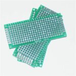
What is a Flexible PCB?
A flexible PCB, also known as an FPC, is a printed circuit board that is designed to be flexible and bendable. Unlike traditional rigid PCBs, FPCs are made using flexible substrate materials such as polyimide or polyester. This flexibility allows them to be used in applications where the circuit board needs to conform to a specific shape or withstand repeated bending and flexing.
Advantages of Flexible PCBs
Flexible PCBs offer several advantages over their rigid counterparts:
- Space-saving: FPCs can be bent and folded to fit into tight spaces, making them ideal for compact electronic devices.
- Lightweight: The thin and flexible nature of FPCs reduces the overall weight of the electronic assembly.
- Durability: FPCs can withstand repeated bending and flexing without damage, ensuring long-term reliability.
- Improved signal integrity: The shorter trace lengths and reduced parasitic capacitance in FPCs lead to improved signal integrity.
- Cost-effective: FPCs can simplify the assembly process and reduce the number of connectors required, resulting in cost savings.
Flexible PCB Manufacturing Process
The flexible PCB manufacturing process involves several critical steps that ensure the quality and reliability of the final product. Let’s explore each step in detail.
Step 1: Design and Artwork Creation
The first step in the flexible PCB manufacturing process is designing the circuit and creating the artwork. This involves using specialized PCB design software to lay out the circuit diagram, component placement, and trace routing. The design must take into account the flexibility requirements, bend radius, and material properties of the FPC.
Step 2: Material Selection
Once the design is finalized, the next step is to select the appropriate materials for the flexible PCB. The most commonly used substrate materials for FPCs are polyimide and polyester. Polyimide is known for its excellent thermal stability, chemical resistance, and mechanical properties, making it suitable for high-reliability applications. Polyester, on the other hand, is more cost-effective and is often used in less demanding applications.
Step 3: Lamination
The lamination process involves bonding the conductive copper layer to the flexible substrate material. This is typically done using adhesive or adhesiveless methods. In the adhesive method, a layer of adhesive is applied between the copper foil and the substrate, and the layers are laminated together under heat and pressure. In the adhesiveless method, the copper foil is directly bonded to the substrate without the use of an adhesive.
Step 4: Drilling and Punching
After lamination, the next step is to create holes and openings in the FPC for component mounting and interconnections. This is done using precise drilling and punching techniques. Laser drilling is often used for creating small, high-precision holes, while mechanical drilling is used for larger holes. Punching is used to create custom shapes and outlines in the FPC.
Step 5: Patterning and Etching
Once the holes and openings are created, the next step is to pattern the copper layer to create the desired circuit traces. This is typically done using photolithography and etching processes. A photoresist layer is applied to the copper surface and exposed to UV light through a photomask that contains the circuit pattern. The exposed areas of the photoresist are then developed and removed, leaving the desired circuit pattern exposed.
The exposed copper is then etched away using a chemical etching process, leaving only the desired circuit traces on the substrate. The remaining photoresist is then stripped away, revealing the final circuit pattern.
Step 6: Surface Finish
After the circuit pattern is formed, a surface finish is applied to the copper traces to protect them from oxidation and improve solderability. Common surface finishes for FPCs include:
- ENIG (Electroless Nickel Immersion Gold): A layer of nickel is deposited on the copper traces, followed by a thin layer of gold. ENIG provides excellent solderability and durability.
- OSP (Organic Solderability Preservative): A thin, organic coating is applied to the copper traces to prevent oxidation. OSP is a cost-effective option but has a limited shelf life.
- Immersion Silver: A thin layer of silver is deposited on the copper traces, providing good solderability and low cost.
- Immersion Tin: A thin layer of tin is deposited on the copper traces, offering good solderability and low cost.
Step 7: Solder Mask Application
A solder mask is a protective coating applied to the FPC to prevent solder bridging and protect the circuit from environmental factors. The solder mask is typically applied using screen printing or photoimaging techniques. Openings are created in the solder mask to expose the pads for component soldering.
Step 8: Silkscreen Printing
Silkscreen printing is used to add text, logos, and other markings to the FPC for identification and assembly purposes. The silkscreen ink is applied using a screen printing process and then cured to ensure durability.
Step 9: Cutting and Profiling
Once all the fabrication processes are complete, the FPC needs to be cut and profiled to its final shape and size. This is typically done using precision cutting methods such as die-cutting or laser cutting. The cutting process must be carefully controlled to ensure the FPC maintains its flexibility and does not suffer from any damage or delamination.
Step 10: Electrical Testing and Inspection
The final step in the flexible PCB manufacturing process is electrical testing and inspection. Each FPC undergoes rigorous testing to ensure it meets the specified electrical and mechanical requirements. This includes continuity testing, insulation resistance testing, and visual inspection for any defects or anomalies.
Quality Control in Flexible PCB Manufacturing
Ensuring the quality and reliability of flexible PCBs is crucial for their successful application in various industries. Quality control measures are implemented throughout the manufacturing process to identify and rectify any issues. Some key quality control aspects include:
- Material inspection: Incoming materials, such as substrates and copper foils, are inspected for thickness, purity, and consistency to ensure they meet the required specifications.
- In-process inspection: Visual inspections and automated optical inspection (AOI) systems are used to monitor the quality of the FPC at various stages of the manufacturing process. This helps identify any defects or deviations early on.
- Electrical testing: Comprehensive electrical testing, including continuity testing and insulation resistance testing, is performed to verify the electrical integrity of the FPC.
- Environmental testing: FPCs may be subjected to environmental testing, such as temperature cycling and humidity testing, to ensure they can withstand the intended operating conditions.
- Traceability: Each FPC is assigned a unique identifier to enable traceability throughout the manufacturing process and in the event of any quality issues.

Challenges in Flexible PCB Manufacturing
While flexible PCBs offer numerous benefits, their manufacturing process presents some unique challenges compared to rigid PCBs. Some of these challenges include:
- Material handling: The thin and flexible nature of FPCs requires careful handling to prevent damage or deformation during the manufacturing process.
- Dimensional stability: Ensuring dimensional stability of the FPC during lamination and other processes is crucial to maintain the desired circuit layout and performance.
- Adhesion: Achieving reliable adhesion between the copper foil and the flexible substrate is critical to prevent delamination and ensure long-term reliability.
- Bend radius: Designing and manufacturing FPCs with the appropriate bend radius is important to prevent damage and ensure reliable operation in the intended application.
- Conductive inks: Selecting and processing conductive inks for flexible PCBs can be challenging due to the different thermal and mechanical properties compared to traditional copper traces.
Here is a table summarizing the key steps in the flexible PCB manufacturing process:
| Step | Description |
|---|---|
| Design and Artwork Creation | Creating the circuit design and artwork using PCB design software. |
| Material Selection | Selecting the appropriate flexible substrate material (polyimide or polyester). |
| Lamination | Bonding the conductive copper layer to the flexible substrate using adhesive or adhesiveless methods. |
| Drilling and Punching | Creating holes and openings in the FPC for component mounting and interconnections. |
| Patterning and Etching | Forming the desired circuit pattern on the copper layer using photolithography and etching. |
| Surface Finish | Applying a protective surface finish to the copper traces (ENIG, OSP, Immersion Silver, or Immersion Tin). |
| Solder Mask Application | Applying a solder mask to protect the circuit and prevent solder bridging. |
| Silkscreen Printing | Adding text, logos, and markings to the FPC using silkscreen printing. |
| Cutting and Profiling | Cutting and profiling the FPC to its final shape and size. |
| Electrical Testing and Inspection | Conducting electrical testing and inspection to ensure the FPC meets the required specifications. |
Frequently Asked Questions (FAQ)
- What is the difference between a flexible PCB and a rigid PCB?
-
A flexible PCB is designed to be bendable and can conform to various shapes, while a rigid PCB is a solid, non-flexible board. Flexible PCBs use flexible substrate materials like polyimide or polyester, whereas rigid PCBs typically use FR-4 or other rigid substrates.
-
What are the advantages of using flexible PCBs?
-
Flexible PCBs offer several advantages, including space savings, lightweight construction, improved durability, enhanced signal integrity, and cost-effectiveness. They can be bent and folded to fit into tight spaces and withstand repeated flexing without damage.
-
What materials are commonly used for flexible PCBs?
-
The most commonly used substrate materials for flexible PCBs are polyimide and polyester. Polyimide offers excellent thermal stability, chemical resistance, and mechanical properties, while polyester is more cost-effective and suitable for less demanding applications.
-
How are flexible PCBs manufactured?
-
The flexible PCB manufacturing process involves several steps, including design and artwork creation, material selection, lamination, drilling and punching, patterning and etching, surface finish application, solder mask application, silkscreen printing, cutting and profiling, and electrical testing and inspection.
-
What are the challenges in manufacturing flexible PCBs?
- Manufacturing flexible PCBs presents some unique challenges, such as material handling, ensuring dimensional stability, achieving reliable adhesion between layers, designing appropriate bend radii, and selecting and processing conductive inks. These challenges require specialized equipment, processes, and expertise to overcome.
Conclusion
Flexible PCBs have revolutionized the electronics industry by enabling the development of compact, lightweight, and durable electronic devices. The flexible PCB manufacturing process involves a series of intricate steps, from design and material selection to lamination, patterning, and testing. Understanding the nuances of each step is crucial for ensuring the quality and reliability of the final product.
As technology continues to advance, the demand for flexible PCBs is expected to grow, driven by the increasing miniaturization and functionality of electronic devices. Manufacturers must stay abreast of the latest advancements in materials, processes, and equipment to meet the evolving requirements of industries such as consumer electronics, automotive, aerospace, and medical devices.
By mastering the art of flexible PCB manufacturing, companies can unlock new possibilities in product design, performance, and reliability. With the right expertise and attention to detail, flexible PCBs will continue to shape the future of electronics, enabling the development of innovative and game-changing devices that push the boundaries of what is possible.

