Introduction
Lasers have become an indispensable tool in the manufacturing of printed circuit boards (PCBs). The highly focused coherent beam of laser light can be leveraged in many ways during the PCB fabrication process to enable precision features and streamline production.
This article provides an overview of the key applications where laser technology is transforming PCB manufacturing:
- Laser drilling
- Direct imaging
- Laser etching
- Laser cutting
- Laser depaneling
- Laser testing
- Microvia formation
Continue reading for an in-depth look at how lasers are driving innovation across the entire PCB production workflow.
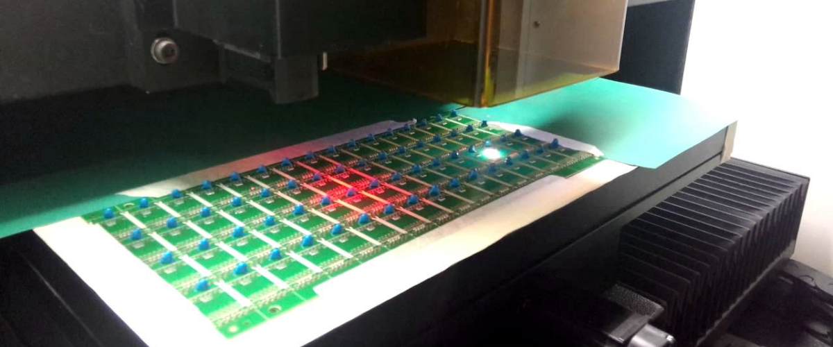
Laser Drilling
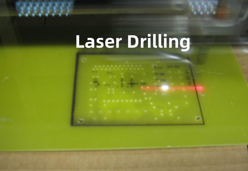
One of the most widespread uses of lasers in PCB fabrication is for drilling small holes used to make interconnections between layers.
Key advantages of laser drilling:
- Diameters down to 25-30 μm are possible
- High accuracy and precision
- Minimal smearing and debris
- No mechanical contact or tool wear
- Suitable for fragile or flexible materials
- Very high throughput of up to 100,000 holes per second
<img src=”https://drive.google.com/uc?export=view&id=1Am9E_9lTg1o7OdnbUGFZbnrSAeqxTNW3″ alt=”Laser drilling PCBs” style=”width:500px;height:300px;”>
These benefits make laser drilling ideal for high density interconnect (HDI) PCBs which require large numbers of tiny closely spaced holes known as microvias. The most widespread industrial laser used is the CO2 laser with a 10.6μm wavelength.
Direct Imaging
Lasers can directly transfer circuit patterns onto photosensitive layers during PCB fabrication without the need for physical masks:
Benefits of laser direct imaging (LDI):
- Eliminates master tooling like films or plates
- Allows rapid design changes without mask revisions
- Ideal for quick-turn prototyping requiring design tweaks
- Reduces costs associated with tools and storage
- Environmentally cleaner process
<img src=”https://drive.google.com/uc?export=view&id=1FTFj1-NpeGCNo_ID5gaHmMR9LDQ7oZa3″ alt=”Laser direct imaging PCB” style=”width:500px;height:300px;”>
With its flexibility and responsiveness, LDI using laser plotters has become the dominant imaging technology for PCB production.
Laser Etching
Lasers can selectively remove copper from predefined areas on a PCB to create circuit traces in a process called laser etching:
Advantages of laser etching:
- Non-contact, no tooling wear or breakage
- Eliminates etching chemicals
- Reduced process steps
- Scalable and cost-effective
- Suitable for quick-turn or low volume jobs
- Allows post-etch modifications
Laser etching provides an environmentally cleaner alternative to traditional chemical etching for forming traces, especially suited for advanced PCBs with thinner copper and delicate structures.
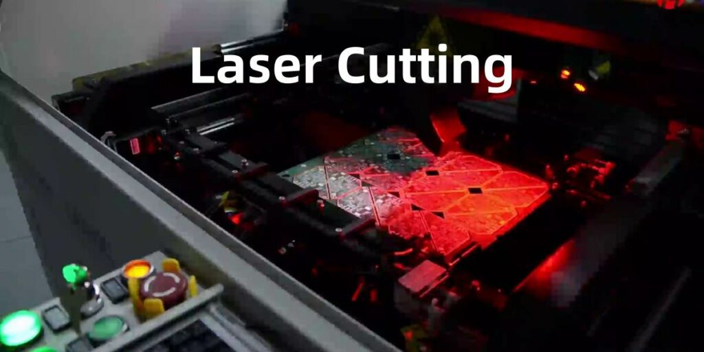
Laser Cutting
Lasers offer contactless, precision cutting of PCB substrate material and sheets:
Benefits of PCB laser cutting:
- Rapid, accurate cutting of intricate profiles
- Minimal heat affected zone
- No mechanical stresses or tool wear
- High uptime with low maintenance
- Cleaner process with no liquids
- Can cut challenging materials like ceramics
Laser cutting allows handling of even the most delicate flexible and brittle boards with minimal defects or damage.
Laser Depaneling
Individual PCBs must be cut apart from larger panels used for mass production:
Advantages of laser depaneling:
- High speed separation of strange board shapes
- Minimal kerf width as low as 100μm
- Reduces stress on boards from blade cutting
- No debris or particulates
- Suitable even for ultra-thin flex boards
- Can cut panels with mounted components
Laser depaneling improves efficiency and yield while minimizing damage to delicate PCBs.
Laser Testing
Lasers can be used for non-contact PCB inspection and testing:
Laser testing techniques:
- Laser voltage probing – contactless voltage measurements
- Thermal mapping – imaging thermal characteristics
- Signal analysis – tracing waveform activity
- Fault isolation – detecting shorts and opens
- Counterfeit detection – verifying component authenticity
- Barcode reading – product identification
Laser testing provides detailed PCB characterization and fault analysis without physical connections.
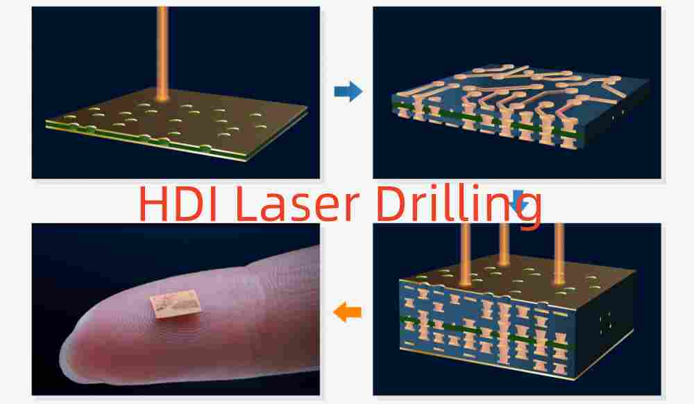
Microvia Formation
Small interlayer holes called microvias electrically connect adjacent layers in high density PCBs. While mechanical drilling can make holes down to ~150μm, only lasers can achieve true microscale vias:
Laser microvia capabilities
- Diameters down below 50μm
- Depth control in micron increments
- Conical shape improves aspect ratio
- Allows 4-10x increased connection density
- Enables multilayer HDI PCBs for miniaturization
Only laser drilled microvias provide the interconnection density needed for emerging applications like 5G communications, high speed computing, advanced driver assist systems, wearables etc.
Laser Types Used
Different laser types are uniquely suited for particular PCB manufacturing applications:
- CO2 lasers (10.6μm) – Drilling, via formation, cutting
- Nd:YAG lasers (1.06μm) – Microvia drilling, imaging, depaneling
- UV lasers (355nm) – Direct imaging for cationic photoresists
- Picosecond lasers – Precise ablation for flex PCBs
- Fibre lasers (1.5μm) – Fine feature etching, drilling
Matching the laser wavelength, pulse properties, beam characteristics and parameters to each fabrication process ensures optimal results.
Conclusion
The unique properties of laser light are being leveraged for a diverse array of PCB manufacturing applications from drilling and imaging through testing and micro-machining. Laser-based techniques enable reaching finer resolutions and higher accuracies while improving productivity across the fabrication workflow. As PCB technology advances to meet the needs of next-generation electronics in areas like mobility, IoT and communications, innovative laser processes will be indispensable for achieving the required speed, precision, density and quality. While lasers do require significant capital investment, their long-term benefits make them a truly transformative tool for the future of PCB manufacturing.
FAQs
What are some limitations in using lasers for PCB fabrication?
Laser methods can have lower throughput than mechanical processes for some tasks. Running costs and maintenance are higher than traditional tools. Significant operator skill is required. Thermal damage must be minimized through proper parameters.
How does the wavelength impact laser drilling characteristics?
Shorter UV wavelengths provide finer resolution but have lower penetration. Longer IR wavelengths drill deeper vias but have lower precision. Configuration, pulse width, fluence all also impact quality.
What accuracy is achievable with laser direct imaging?
With high precision stages and optics, alignment accuracy better than 10μm is achievable allowing very fine traces comparable to phototools. Vibration control is critical.
Why is laser depaneling preferred over mechanical routing?
Laser depaneling avoids mechanical stresses, debris, tool wear or breakage. It prevents micro-cracks and damage to boards or components. No subsequent cleaning required.
What are some key application areas driving adoption of laser-based PCB manufacturing?
High density interconnect PCBs, flexible circuits, advanced packaging, 5G modules, heterogeneous integration, miniaturized electronics.


