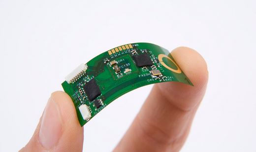
A printed circuit board (PCB) is a thin board made of fiberglass, composite epoxy, or other durable insulating materials. PCBs serve as the base for etched copper pathways and provide mechanical support and electrical connections between electronic components using conductive pathways, traces, pads and junctions etched from copper sheets laminated onto the non-conductive substrate.
PCBs provide numerous advantages over traditional point-to-point construction methods including:
- More reliable and consistent electronic performance
- Higher component density and complexity while reducing size and weight
- Lower production costs at scale
- Improved ease of manufacture and servicing
With these benefits, PCBs have become ubiquitous across nearly all modern electronics found in computing, communications, industrial, medical, transportation, scientific and countless other segments.
Major Applications and Uses of PCBs

PCBs are extremely versatile and can be tailored to meet the specific needs of an electronic device or system. Here we explore some of the most common and impactful uses and applications of PCBs.
Computer and Server Motherboards
The motherboard serves as the main PCB inside computers and servers, designed to allocate power from the power supply and enable communication between critical components including the CPU, memory, expansion cards, storage devices and more. Motherboards come in various standardized form factors and layouts depending on the type of device and performance requirements.
Smartphones and Tablets
Mobile consumer electronics like smartphones and tablets also rely heavily on PCBs to integrate the main processor, wireless modems and antennas, memory chips, sensors, charging and peripheral ports, screens and other components into compact and robust mobile devices. Phone PCBs must also be engineered to be very power efficient to preserve battery life.
Telecommunications Infrastructure
Within telecom systems like cellular base stations, switches, routers and transmission gear, high performance PCBs enable routing and processing of voice, data, radio and optical signals. Reliability is paramount so rigid, high frequency PCB materials are used.
Figure 3. Advanced multi-layer PCBs are required to meet the signal integrity needs in high speed telecom systems.
Automotive Electronics
Cars have evolved to become sophisticated computing platforms on wheels. Automotive PCBs have to survive under the hood heat and vibration while providing engine monitoring and control, transmission and chassis management, GPS navigation, backup cameras, vehicle-to-vehicle communications, ADAS self-driving sensors, EV battery management systems, infotainment and more recently vehicle-to-everything (V2X) connectivity.
Industrial Electronics
To control sensitive manufacturing processes, achieve precision motion control, monitor production systems health and enable advanced robotics, a wide array of industrial electronics leverage specialty PCBs rated to handle more extreme temperatures, voltages, vibration, contamination and other environmental factors. Field Programmable Gate Array (FPGA) and microcontrollers are frequently employed to allow flexibility.
Figure 5. Rugged PCBs find use across industrial environments with more extreme temperature, contamination, vibration and interference.
Medical Devices
Within advanced medical, surgical and therapeutic devices, PCBs enable touchscreen interfaces, wireless connectivity, battery charging, power supplies, sensors to track patient vitals, pumps, valves, motors, product safety supervisors and much more. Medical PCBs emphasize maximum safety and reliability given life critical applications.
IoT and Wearable Products
The rise of consumer IoT and wearable technology including smart watches, fitness trackers, home automation controls, appliances and more relies on extremely compact and low cost PCB solutions to provide the brains behind the connected product operation. Focus is placed on wireless connectivity, ultra low power consumption and security.
PCB Materials, Design and Manufacturing
Many factors determine the type of PCB materials, design practices and manufacturing processes utilized which shape the performance capabilities, mechanical properties, environmental resistance, reliability, producability and cost of the final boards.
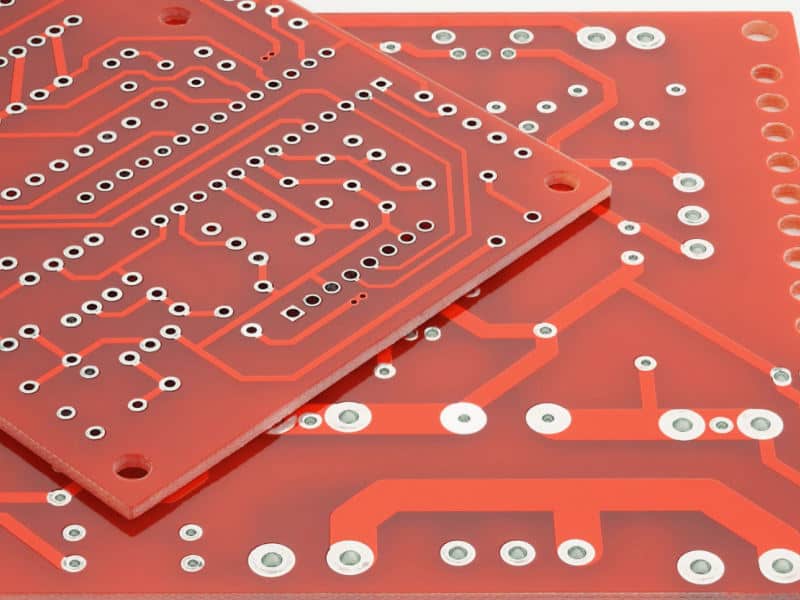
PCB Substrate Materials
The substrate is the base insulating material onto which the conductive copper pathways are etched or deposited. Key substrate properties include dielectric constant (determines signal propagation speed), thermal conductivity, coefficient of thermal expansion and flammability rating. Substrate materials include:
- FR-4 Glass Epoxy – Most common rigid PCB material, good manufacturability/value
- CEM-1 Cotton Paper – Common low-cost rigid PCB material
- FR-2 Phenolic – Lesser used rigid PCB good for lower frequencies
- Polyimide – Advanced rigid/flex PCB material capable of very high temperatures
- PTFE – Specialty rigid PCB material for microwave and mmWave circuits
Layer Count
Single sided PCBs have copper traces on one side only, double sided has conductor layers on both sides. More complex boards can incorporated 30 or more layers interconnected with plated through hole vias or other vertical interconnect technologies. High layer counts enable increased functionality and component density.
Conductor Thickness
Common copper thicknesses range from 0.5 oz (0.0007 inches) up to 6 oz (0.0042 inches) or more. Thicker copper is lower resistance but comes at increased material costs. High current applications require very thick copper to avoid overheating.
Minimum Trace Width/Spacing
The resolution of the etched copper traces and spacing between them determine the component density and complexity possible. State of the art PCB fabricators can achieve trace widths and spaces down to 3 mils (0.003 inches).
Via Styles
Vertical interconnect access (VIAs) extend connections between layers. Common via types include through hole vias (drilled hole with copper plating), blind vias (connect inner layers only) and buried vias (contained between inner layers). Microvias (<0.15mm diameter) allow stacking of connections.
Surface Finishes
The copper surface finish plays a large role in solderability and preventing oxidation/corrosion. Common finishes include organic solderability preservative (OSP), immersion silver, immersion tin, gold plating. Lead-free requires improved finish.
PCB Design Software
Engineers use sophisticated PCB design automation tools for schematic capture, simulation/verification and board layout with integrated rules on trace widths, component clearances, high speed topology, signal integrity and manufacturability constraints.
CAM and Gerber Files
Finished board designs are converted into a set of instructions for board fabrication and assembly called gerber files which unambiguously define drill locations, copper layers, solder masks, silkscreens, etc.
PCB Manufacturing Process
To fabricate blank PCBs suitable for population with components, batches of boards progress through an array of complex processes including:
- Imaging – Photoresist laminated onto copper layers
- Exposure – Defines circuit pattern onto photoresist using phototools
- Developing – Dissolves unexposed photoresist
- Etching – Removes copper not protected by resist
- Stripping – Removes remaining photoresist
- Drilling – Machines holes for vias
- Plating – Electrolytic copper plating makes holes conductive
- Routing – Trims exterior board dimensions
- Testing – Verifies quality of bare boards
- Population – Solders components onto finished PCB
Environmental Responsibility
With electronics more ubiquitous across modern life, sustainability through the product lifecycle is crucial including responsible design, use of less hazardous materials, extended product lifetime through repair/reuse, and improved end of life recycling programs to recover valuable resources to minimize waste and exposure.
The Future of Electronics and PCBs
The electronics industry continues rapid advancement with increased performance, complexity, functionality and intelligence across nearly all segments from consumer gadgets to data center servers to transportation. PCBs will evolve in parallel to enable embedding of more components, higher density interconnect at lower power budgets and smaller sizes.
Uses of PCB FAQ
What are some additional specialized uses of PCBs beyond consumer electronics?
Some additional unique application areas for PCB technology include aerospace avionics, radio frequency identification (RFID) tags enabling wireless inventory management, daylight readable flat panel displays like those in phones and watches, gift/loyalty smart cards, advanced power inverters and motor controllers, crypto mining hardware accelerators and niche research instruments.
What are some key considerations in designing a PCB?
Critical design aspects include appropriate selection of PCB materials to meet reliability, thermal, frequency, cost and manufacturability requirements. Careful floorplanning guides placement and routing to achieve signal integrity and avoid interference while maximizing density. Component footprints must match datasheets. Design for thermal heat spreading, ventilation and adequate power delivery prevents overheating. Test points aid debugging.
Can PCBs support high voltage applications?
Yes, provided proper layout, spacing, insulation, shielding and component ratings are observed. Applications like electric vehicle (EV) battery packs and charging stations, power distribution, renewable inverters and industrial motors operate at dangerously high DC or AC voltages from 50V up to 1kV. Safety standards provide human contact limits. Mixed signal situations require isolation techniques.
What is HDI technology and what problems does it solve in PCBs?
High density interconnect (HDI) allows packing of components and connections beyond normal density limits by employing microvias and often blind/buried vias in thinner dielectric layers paired with thinner circuit traces on outer layers. This reduces layer count for a given level of integration and allows higher frequency performance crucial in cell phones.
How are PCB failure rates predicted and quantified to ensure adequate product reliability?
Statistical modelling leverages techniques like MIL-HDBK-217 to quantify failure rates for PCB assembly materials, fabrication details, part counts, temperatures, environmental stresses and other factors. Results determine field replacement rates and warranty costs. Techniques like HALT (highly accelerated life testing) verification accelerate testing to uncover weaknesses.


