Introduction
A PCB printer is a device used to create printed circuit boards (PCBs) by depositing conductive and dielectric materials onto a substrate. It builds up layers of materials to form the circuits, traces, pads, and other features required on a PCB. PCB printers represent the latest technology in rapid prototyping and agile PCB fabrication.
PCB printers allow designers to quickly iterate and test their designs before finalizing a board for production. They are extremely useful for verifying designs, performing design for manufacturing analysis, creating small batches of customized boards, and enabling on-demand PCB manufacturing.
This article provides a comprehensive overview of PCB printers. It covers:
- How PCB printers work
- Different types of PCB printers
- Materials used in PCB printers
- Advantages and disadvantages of PCB printers
- PCB printer technology comparison
- Applications of PCB printers
- Future trends and outlook
How Do PCB Printers Work?
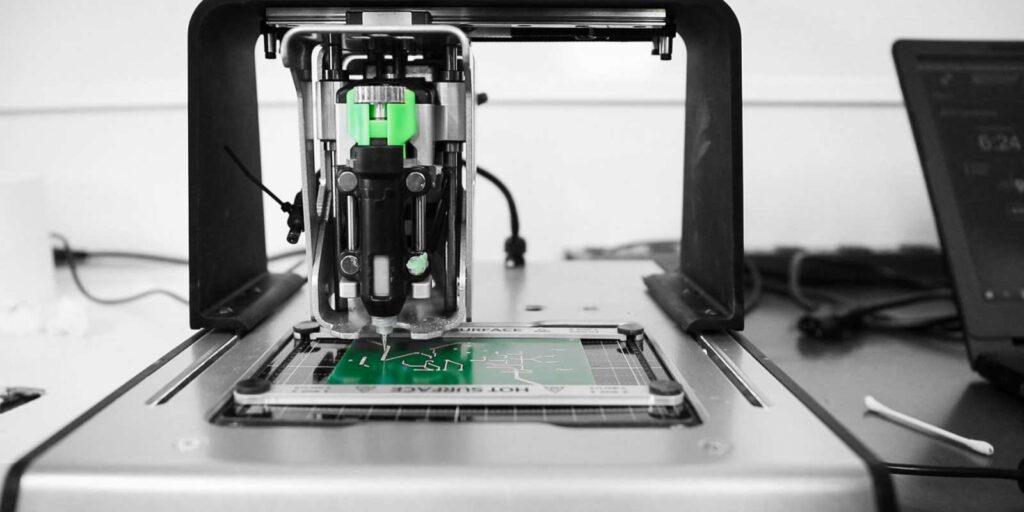
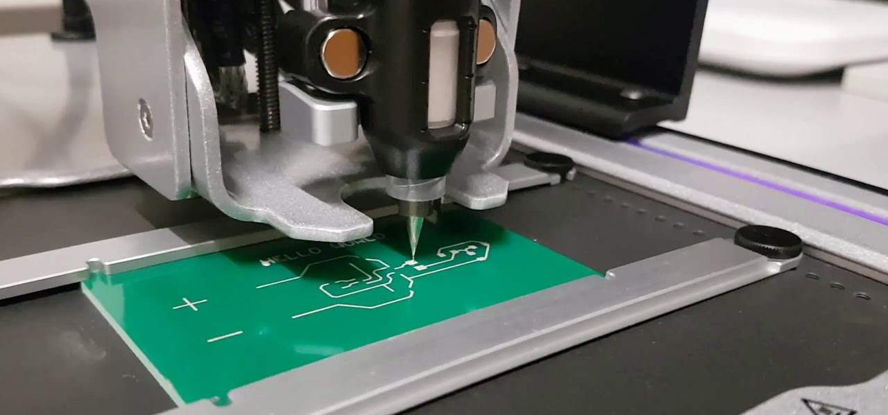
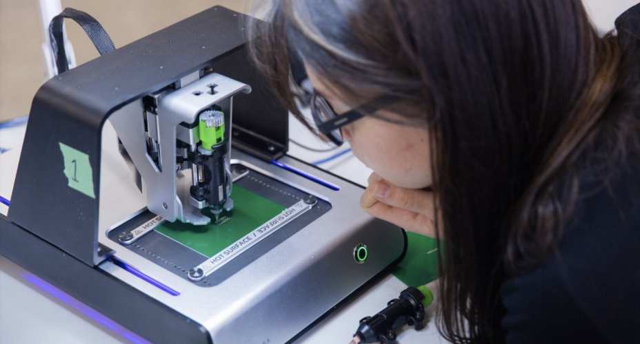
PCB printers work similarly to desktop inkjet or laser printers. They deposit material layer-by-layer and build up the board additively. However, instead of ink or toner, PCB printers deposit conductive and insulating materials to create the board circuitry and structure.
The basic PCB printing process involves:
- Importing the PCB design file generated from CAD software. Common file formats are Gerber, DXF, and IPP.
- The design file is digitally sliced into thin layers, usually around 10-100 microns thick.
- The printer preps the substrate, which is often a rigid PCB material like FR4, Rogers, polyimide, etc. For flexible PCBs, polyimide or PET film is used.
- The print head moves across the substrate, depositing tiny droplets of material according to the first layer in the design file.
- Materials are cured or solidified, often by a UV light integrated into the print head.
- The build platform lowers, and the next layer is deposited on top of the first. The droplet pitch precision is around 20-30 microns.
- This process repeats until every layer has been deposited and a complete PCB is formed. A PCB can have 2-30 layers depending on design complexity.
- Any support structures are removed and the board is cleaned and prepared for post-processing.
Many PCB printers are fully automated and allow unattended “lights-out” operation 24/7. Overall, the process is similar to 3D printing but with different materials suited for PCB fabrication.
PCB Printing Process (Image Credit: Nano Dimension)
Types of PCB Printers
There are several technologies used in PCB printers today. Each has its own unique capabilities, advantages, and limitations.
Inkjet PCB Printers
Inkjet PCB printers work by propelling tiny droplets of conductive and dielectric inks from print head nozzles onto a substrate. The inks contain silver, copper, or other metal nanoparticles suspended in a liquid carrier. Once deposited, the inks are cured into solid conductive traces by heat or UV light.
Inkjet printers can produce extremely fine features down to around 10 microns, perfect for complex PCBs and semiconductor packaging. However, the cured traces have higher resistance compared to traditional copper. Also, inkjet printing relies more on surface tension for precise drop placement rather than direct mechanical control.
Major companies with inkjet PCB printer technology include:
- Neotech AMT
- Novacentrix PulseForge
- Fuji Dimatix Materials Printer
- Optomec Aerosol Jet Printer
Aerosol Jet PCB Printers
Aerosol jet printing uses an atomized mist of nanoparticle inks that are aerodynamically focused onto the print area. This allows printing features down to around 10 microns in width. The ink particles are deposited directly via the gas stream rather than liquid droplets.
Aerosol jet can print highly complex conductor patterns and overcomes some limitations of liquid inkjet. It provides tighter process control and can use a wider range of inks. The downside is the slower speed and smaller build area compared to other printers.
Key companies with aerosol jet capabilities are Optomec and Prismo.
Photolithography PCB Printers
Photolithography mimics traditional PCB manufacturing using light to pattern board layers. A liquid photoresist is deposited, exposed to collimated UV light through a mask, and developed to remove unwanted areas. Conductors and insulators are added in the exposed areas.
While the process is slower, it can produce extremely high resolution (down to 1 micron) and accurate traces with the conductivity of pure copper. Photolithography printers are made by companies like Lithoz, NanoSystem, and Racyics.
Extrusion / Dispensing PCB Printers
Material extrusion printers use a syringe or piston mechanism to directly extrude conductive traces and dielectric layers onto a substrate. Materials flow out of a nozzle as the print head traces over the board. Once deposited, the materials self-level and solidify instantly.
These printers are relatively low cost and support a wide range of materials including silvers, dielectrics, polymers, ceramics, and solder pastes. Resolution is around 100 microns. Major companies are Nano Dimension, Voltera, BotFactory, and Voxel8.
Hybrid PCB Printers
Some advanced PCB printers combine multiple technologies together into one system. For example, the Inkbit Vista system uses inkjet printing along with photolithography and material jetting. This hybrid approach allows integrating the strengths of each process.
Other printers may combine inkjet with pick-and-place assembly to add surface mount components during printing. This provides fully additive PCB fabrication in a single compact machine.
PCB Printer Materials
PCB printers utilize conductive inks, pastes, and other specialty materials to build up circuit layers. Here are some of the common materials used:
- Silver – nanoparticle silver inks are used to print highly conductive traces and features. Most inkjet and aerosol jet printers use silver-based inks.
- Copper – while harder to print with, copper offers the best conductivity. Some photolithography printers can deposit copper.
- Dielectrics – various insulating polymers and other dielectrics are printed between conducting layers.
- Solder – solder paste extrusion allows depositing pads, bumps, and through-hole metallization.
- Adhesives – adhesive printing adheres components and seals layers.
- Specialty materials – printers can also utilize exotic materials like graphene, carbon nanotubes, proteins, etc.
The performance, processing, and properties of these materials are critical to printing resolution, electrical characteristics, and reliability of the PCB. Extensive R&D is underway to expand material capabilities.
Benefits of PCB Printers
Here are some of the major advantages that on-demand PCB printers offer over traditional PCB fabrication:
Fast prototyping – PCB printers allow designing, iterating, and testing boards rapidly without long turnaround times. Changes can be printed in hours vs weeks for fabrication.
Low volume production – Economical short-run manufacturing. Print 5-50 boards instead of high minimum orders from PCB fabs.
Design flexibility – Freeform tools enable innovative board shapes and traces. Embedded components too.
Simplified workflow – Eliminate DFM issues. Print directly from CAD and avoid generating Gerbers, drilling, etc.
On-demand fabrication – Produce boards when needed instead of waiting for batches. Supports agile development.
IP protection – In-house printing protects sensitive designs. No need to share IP with external fabricators.
Cost saving – Lower costs compared to high mix/low volume fabrication charges. Also saves on repeated prototyping costs.
Sustainability – Additive printing with minimal waste vs traditional subtractive PCB processes with chemicals.
Limitations of Current PCB Printers
While PCB printers have many benefits, they also have some limitations in their current stage of technology evolution. Some of these include:
- Limited substrate size – Most printers max out around 9″x12″ or 22cm x 30cm. Insufficient for larger designs.
- Lower throughput – Print speed is still much slower than mass PCB fabrication. Not yet viable for high volume production.
- Lower electrical performance – Printed traces have higher resistivity than copper. Also greater noise and impedance variability.
- Limited resolution – printers range from 1 to 100 microns line width, but lower end of range is very slow. Limits component density.
- Fewer material choices – Limited conductive, dielectric, and packaging materials available compared to the wide selection used in industry PCB fabrication processes.
- Lower reliability – questions remain about thermal cycling, mechanical strength, moisture resistance, etc. especially for mission-critical or high performance products.
- Surface finish – harder to achieve soldermask and surface finishes inline. Often requires secondary post-processing.
- Via formation – printing conductive vias remains challenging. Construction, alignment, and aspect ratio are limiting factors.
PCB Printer Technology Comparison
Here is a detailed comparison of the major PCB printer technologies available:
| Parameter | Inkjet | Aerosol Jet | Photolithography | Extrusion |
|---|---|---|---|---|
| Resolution | 10 microns | 10 microns | 1 micron | 100 microns |
| Line Width | 10-50 um | 10-50 um | 1-20 um | 100-500 um |
| Layer Height | 1-5 um | 1-5 um | 25-100 um | 10-100 um |
| Print Speed | Low-Medium | Low | Low | Medium-High |
| Materials | Silver & copper inks | Wide material range | Photoresists, copper | Pastes, silver inks, polymers |
| Layer Registration | Medium | Medium-High | Very High | Medium |
| Minimum Feature Size | 50 um | 50 um | 15 um | 500 um |
| Circuit Density | High | High | Very High | Low |
| Electrical Performance | Medium | Medium | High | Medium |
| Substrate Size | Small | Small | Medium | Medium |
| Process Complexity | Low | High | High | Low |
| Initial System Cost | Medium | Very High | High | Low |
| Operating Cost | Medium | High | Medium | Low |
Resolution
Photolithography can achieve extremely high 1 micron resolution while extrusion printers are limited to around 100 microns. Other methods fall in the 10-50 micron range.
Registration
Photolithography and aerosol jet have the best layer-to-layer alignment accuracy critical for multi-layer boards.
Speed
Extrusion is the fastest for larger traces while photolithography and inkjet are slower but higher precision.
Cost
Inkjet and extrusion printers have lower initial system costs. Photolithography and aerosol jet printers often cost over $100,000. Operating costs are also lower for inkjet and extrusion printers.
Applications of PCB Printers
Here are some of the most common applications where PCB printers deliver significant value:
Prototyping – Allows engineers to rapidly iterate on designs and test concepts before starting production. Faster feedback and development.
Low volume production – For small batches between 5-100 boards, printing is more economical than traditional fabrication. Useful for custom boards.
R&D – Enables innovation in designs, materials, and fabrication processes. Flexible tools for R&D.
Education – Provides hands-on experience with PCB design/manufacturing. Trains students on state-of-the-art processes.
Custom / unique designs – Printers can produce complex and compact PCBs that would be infeasible with standard methods.
On-demand fabrication – Boards can be manufactured on the fly in hours versus days or weeks. Critical spares and repairs.
Rapid design modifications – Design changes can be printed quickly without re-spins or new tooling.
IP protection / ITAR – Internal printer keeps designs secret and avoids sending to external PCB shops.
3D electronics – Conformal and embedded electronics via printing directly onto 3D surfaces.
Biomedical devices – Print flexible circuits directly on medical devices like implants or wearables.
Smart objects – Embed intelligence in products by printing circuits onto toys, consumer goods, structure, etc.
Future Outlook
PCB printers are still an emerging technology but the outlook is very positive with rapid advancement on multiple fronts:
- Increasing resolution and feature sizes – Expect finer features rivalling traditional processes as printer technology improves.
- Better electrical performance – Conductivity and reliability will approach that of standard PCBs thanks to material science innovations.
- Faster print speeds – Throughput will increase significantly enabling true mass production via printing.
- Expanding printer portfolio – More printer manufacturers with broader range of sizes, speeds, resolutions, and technologies tailored to diverse applications.
- Hybrid manufacturing integration – Printers will integrate with pick-and-place, surface mount assembly, inspection, and other backend processes for complete in-house production.
- Mainstream adoption – The industry is increasing awareness and acceptance of PCB printing as performance reaches “good enough” thresholds.
- Cost reductions – Economies of scale will reduce both printer costs and material costs as demand increases adoption across segments.
- New applications – We will see PCB printing spread into sectors like medical, aerospace, defence, and automotive pushing the technology further.
With so many promising developments underway, PCB printing is poised to revolutionize electronics design and manufacturing in the coming decade.
Frequently Asked Questions
Q: How accurate are PCB printers?
PCB printers can achieve accuracy down to around 10 microns, with photolithography being the most precise. Registration between layers is +/- 5 to 10 microns for most printers. This meets the demands of many applications.
Q: Can PCB printers make multilayer boards?
Yes, current PCB printers can produce multilayer boards with up to 30 conductive layers interconnected using printed vias. However, performance may differ from conventionally laminated multilayer boards.
Q: What printer resolution is needed for 0201 components?
0201 components require line widths down to around 100 microns. Photolithography or high resolution inkjet printers with 10 micron sizes can reliably produce traces for 0201 pads and pins.
Q: How do printed vias compare to drilled vias?
Drilled vias can achieve higher aspect ratios with smoother sidewalls. Printed vias have lower aspect ratios and rougher profiles which can impact reliability and plating adhesion.
Q: What secondary processing might be needed after PCB printing?
Post-printing processes like annealing, plating, soldermask application, surface finishing, legend printing, AOI inspection and testing may be required to achieve the necessary electrical, mechanical, and aesthetic properties.
Conclusion
PCB printers represent a revolutionary additive manufacturing approach to creating electronics. By depositing conductive and dielectric materials layer-by-layer, PCB printers can quickly generate boards on demand with no need for layout, masking, imaging, etching, drilling, etc.
While the technology is still evolving, PCB printers are already valued for fast prototyping, design flexibility, customization, and on-demand fabrication. As printer resolution and material performance advance, PCB printing promises to transform the electronics design and manufacturing landscape.


