Overview of Gerber Files
A Gerber file is a file format used to represent printed circuit board (PCB) designs and manufacture their layers. Gerber files are extensively used in PCB fabrication workflows to transfer design data from CAD software to machines that manufacture the boards.
Gerber files contain 2D vector image data of each copper layer, solder mask layer, silkscreen layer, drill data and other aspects of a PCB design. Gerber files are generated by PCB design software when the designer is ready to get their boards fabricated. The complete set of Gerber files contains all the information a PCB manufacturer needs to produce the boards.
The Gerber file format dates back to the early days of the PCB industry. It was developed by a company called Gerber Systems, who specialized in photoplotter machines used to image PCB layers. Although quite old, the Gerber format remains a ubiquitous industry standard for PCB designs today due to its ease of use and reliability.
Understanding Gerber files is crucial knowledge for electronics engineers and hobbyists interested in designing and making their own circuit boards. In this comprehensive guide, we dive into all aspects of Gerber files, from generation to interpretation.
History and Origins
The Gerber file format was invented by Gerber Systems Corporation, a company founded in 1960 by H. Joseph Gerber. Gerber made a photoplotter, the Gerber hijacker, which was an optical machine to image master film for printed circuit board fabrication. It used a beam of light to expose shapes on photosensitive material.
To drive their photoplotter machine, Gerber Systems needed a way to digitally represent PCB images. So their engineers devised the Gerber file format, which contained commands to position the photoplotter’s aperture and expose lines and shapes. The very first version of the Gerber file format was released in 1974.
Once adopted, the usefulness of the Gerber file format spread through the PCB fabrication industry. Even PCB manufacturers using different brand photoplotters could accept Gerber files. It allowed a common transfer language between PCB design software and manufacturing equipment.
Although Gerber has evolved over the years, it remains the de-facto standard for PCB designs today. Almost all PCB CAD systems and fabrication houses use Gerber files in their workflow.
Gerber File Generation

Gerber files are generated from PCB designs using CAD software such as:
- Altium Designer
- Cadence Allegro and OrCAD
- Eagle
- KiCad
- Autodesk EAGLE
Within these CAD programs, the designer first creates the schematic and 2D layout of their circuit board. Components are positioned and the connections routed on various PCB layers.
Once the design is finalized, the designer can export Gerber files corresponding to the layers and manufacturing data:
- Copper layers for the top, bottom etc.
- Solder mask layers that coat the copper
- Silkscreen layer for component markings
- Drill files for holes at component pads
- Profile layer for board outline
- Netlist file for connectivity
- NC drill file for vias and holes
Each layer is exported as an individual Gerber file in the standard format. The full set of Gerber files contains all the vital fabrication and assembly details about that PCB design.
Advanced PCB design software generates industry-compliant Gerber files automatically. But designers can customize the output through Gerber export settings. Parameters like output resolution, file naming, polarity and more can be configured.
Gerber File Format
Gerber files use plain ASCII text to represent PCB images. They consist of commands that instruct a photoplotter or printer how to create shapes, move to locations, expose lines and other graphic actions.
Here are some key aspects of the Gerber file format:
- Each file represents one PCB layer – top copper, bottom copper etc.
- Files use the .gbr extension e.g. bottom_copper.gbr
- Coordinates use inch units by default
- Common commands like D01, D02, D03 define drawing actions
- G04 is a comment and % for file information
- FS, FO define photoplotter flashes for exposing
- AM indicates aperture macro definitions
This is an example of what Gerber file commands look like:

As you can see, it uses simple commands for geometry, comments, aperture definitions and drawing the actual lines and shapes.
Modern Gerber files follow the updated RS-274X standard. It adds enhancements like metric units, improved number precision and aperture macros.
Contents of Gerber File Set
A full set of Gerber files will contain individual files representing all the vital fabrication data about a PCB design. Here are the typical files included:
- Top layer (GTL) – Copper traces on top surface
- Bottom layer (GBL) – Copper traces on bottom surface
- Inner layer (G1-G16) – Copper layers in multi-layer boards
- Top solder resist (GTS) – Solder mask on top layer
- Bottom solder resist (GBS) – Solder mask on bottom layer
- Top silkscreen (GTO) – Component markings etc. for top side
- Bottom silkscreen (GBO) – Component markings etc. for bottom side
- Top solder paste (GTP) – Solder paste layer for SMD pads
- Drill drawing (GD1) – Holes defined as flashes
- NC drill file – Numerically controlled drill file for holes
- Profile layer (GM1) – Outline of finished board shape
- Drill report – Summary table of all drill holes
Additional optional files can include a netlist, testpoints file, and mechanical drawings.
Having all these layers as individual Gerber files provides the PCB manufacturer the full picture to fabricate and assemble the designed circuit board correctly.
Gerber File Viewing and Visualization
Since Gerber files contain ASCII vector graphics commands, they can not be directly opened and viewed like bitmap image formats.
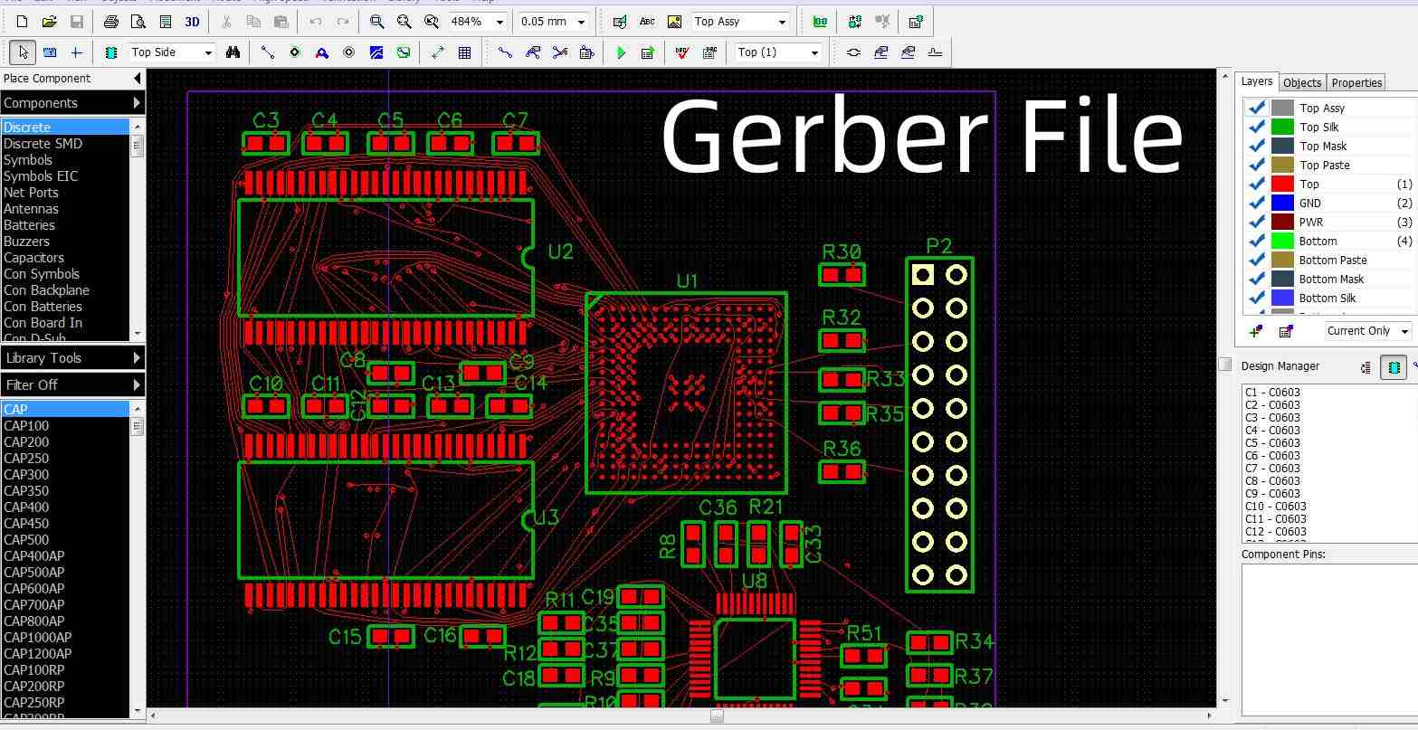
To inspect Gerber files visually, you need to use a Gerber file viewer tool. These tools process the Gerber commands and render them graphically on-screen.
Popular free Gerber viewers include:
- Gerbv – Open-source viewer for Linux and online
- ViewMate – Windows Gerber viewer
- GC-Prevue – Full featured Gerber and NC drill viewer
- LayerViewer – Web-based Gerber viewer
These tools allow designers to zoom in and inspect their Gerbers thoroughly. Features like highlighting unconnected pads, measuring clearances, overlaying layers are extremely useful to verify PCB designs before manufacturing.
PCB CAD software also provides integrated Gerber viewers. This allows checking the exported Gerber files directly within the design tool itself.
Gerber File Validation
Before sending Gerber files off for fabrication, they should always be validated. This step ensures there are no errors that could prevent successful PCB manufacturing.
Typical Gerber checks include:
- Proper file naming conventions followed
- All required layers generated
- Polarity matches across layers
- Correct zero-point reference in files
- No missing copper or aperture definitions
- No unintended open or short circuits
- Solder mask correctly covers copper pads
- Minimum clearance rules followed
- Drill holes aligned at pad centers
The CAM department at fabrication houses performs intensive Gerber validation using specialized software tools. Many offer online Gerber viewers so customers can do basic checks themselves.
Designers should also use Gerber viewers or PCB CAM tools like ODB++ to validate their files thoroughly before releasing to production. This avoids costly mistakes down the line.
Why Gerber Remains the Standard
With technology advancements, why does the decades-old Gerber format still remain the standard for PCB fabrication data? Here are some key reasons:
- Ubiquity – Already adopted across the entire industry
- Reliability – Trusted format proven through years of use
- Simplicity – Based on easy to implement ASCII commands
- Output agnostic – Not tied to any specific machine or printer
- Forward compatibility – Evolving RS-274X standard includes new enhancements
- Ease of troubleshooting – Text format allows identifyingerrors
- Lightweight files – Compact size compared to graphical formats
- Lack of alternatives – No competitor has yet replaced Gerber
Attempts have been made to come up with more modern, graphics-oriented PCB fabrication formats. ODB++ and GenCAD are examples currently making some headway.
However, Gerber’s entrenchment and reliability makes it unlikely to disappear from PCB design workflows anytime soon. It remains the “go-to” format for transferring design intent to physical PCB production.
Gerber File Limitations
While Gerber has many advantages that maintain its dominance, it also has some inherent limitations as an older text-based vector format:
- No standard for layer names – Inconsistent file naming between vendors
- Ambiguity – Certain visual details can be misinterpreted
- Only 2D – No support for 3D mechanical models
- Text representation – Harder to visualize than graphical formats
- Large file sizes – Image repetition results in large files
- Revision tracking – No built-in way to indicate version changes
Due to these factors, small errors can creep into Gerber data if designers are not vigilant. Validation tools and CAM reviews are essential to avoid issues.
As PCB fabrication becomes more complex, growing data demands may eventually motivate a transition to a more robust format than Gerber. But it remains the trusted backbone for now.
The Future of Gerber Files
What does the future hold for the Gerber file format? Here are some possible evolutions:
- Standardization – Industry-wide alignment on updated standards for layer names, polarity etc. This removes ambiguity.
- Compression – Ways to optimize Gerber file sizes without losing data. This reduces storage needs.
- Additional metadata – Support for more metadata like PCB stackup, fabrication notes, EDA tool info etc. embedded right in the Gerber.
- Incremental improvements – More macros, higher precision, additional commands as needed by fabrication technology improvements.
- Hybrid formats – Combining Gerber with XML or database layers to enhance capabilities.
- Graphical encodings – Evolving Gerber to support more graphical constructs rather than pure text.
- Replacement formats – Industry momentum may gradually shift to alternatives like ODB++ if they offer compelling advantages. But unlikely in the short term.
While new formats will emerge, Gerber is still expected to retain its vital place in PCB design workflows for the foreseeable future. The industry knows and understands it well.
Conclusion
Gerber files have been the backbone of PCB designs and manufacturing for decades. This ubiquitous text-based vector format contains layers for every fabrication aspect of a board.
Understanding Gerber file generation, structure and usage is indispensable knowledge for electronics engineers, designers and hobbyists. Even with its limitations, Gerber remains the industry standard for reliable PCB data transfer and production.
With continual improvements in the evolving RS-274X standard, Gerber files will continue playing a key role in translating electronic circuit designs into physical boards far into the foreseeable future.
Frequently Asked Questions
Here are some common questions about Gerber files in PCB design:
Q: Can Gerber files contain 3D model data?
A: No, Gerber files only support 2D PCB layers. For 3D mechanical models and board enclosures, other formats like STEP have to be used.
Q: Do I need to generate every possible Gerber file?
A: You only need to generate Gerber files for the layers used in your PCB design. For simple boards, just top and bottom copper and drill files may suffice.
Q: What is the most common Gerber file error made by designers?
A: The most common issue is incorrect layer polarity settings. This results in mirrored layers that don’t match. Always double check polarity matches across all layers.
Q: Can I open Gerber files in any image editing or vector software?
A: No, Gerber files contain special textual commands rather than graphics. You need to use Gerber viewing software capable of interpreting the commands.
Q: How do I convert Gerber files to standard image formats like PNG?
A: Use Gerber viewing tools to render the design, then export or screenshot the viewport to image formats like PNG. This provides a single flattened graphic of the design.
