Rogers Corporation offers a range of high performance printed circuit board (PCB) materials engineered to meet the needs of radio frequency (RF), microwave and other specialized applications in aerospace, automotive radar, communications, defense and industrial segments.
Proper selection of the Rogers laminates paired with suitable stackups, copper weights, etched trace geometries and fabrication processes enables engineers to achieve precision impedance control, low loss, tight tolerance electrical performance and stability across operating temperature at higher frequencies from MHz into GHz ranges.
Below we outline key considerations and best practices when designing PCBs based on Rogers materials to reap maximum benefit.
Selecting The Right Rogers Material
With over 30 available material options spanning polytetrafluoroethylene (PTFE) composites, ceramic filled, thermoset and thermoplastic formulations, selecting the appropriate Rogers material constitutes the first major design choice.
Factors driving Rogers materials selection include:
- Frequency range (dictates dielectric constant ER and loss tangent)
- Performance consistency needed across temperature
- Layer count requirements and cost targets
- Mechanical traits like flexible vs rigid
- Thermal conductivity to dissipate heat
- Ease of fabrication for line resolution
- Operating environment temperatures
| Material | Dielectric Constant | Loss Tangent | Key Attributes |
|---|---|---|---|
| RO3003TM | 3.0 | 0.0013 | Good performance to GHz range, cost effective |
| RO3006TM | 6.5 | 0.002 | Higher frequency, thermally stable to MongoDB |
| RO3203TM | 3.02 | 0.0016 | Low loss, production ready |
| RO4350BTM | 3.48 | 0.0031 | Glass reinforced, high κ, automotive grade |
| RO4835TM | 3.38 | 0.0021 | Low loss, production ready |
| Table 1. Snapshot of select popular Rogers microwave laminate materials and key specifications. |
Note that dielectrics with higher dielectric constants allow tighter trace spacing and smaller circuits, but suffer more loss at high frequencies. The loss tangent quantifies signal loss.
Modeling and Simulating Rogers PCBs

To ensure the PCB layout achieves target impedance, propagation velocity, reflection and loss parameters vital for high frequency operation, Rogers materials should be modeled and transmission structures simulated within the selected stackup using 3D planar electromagnetic (EM) analysis software such as Keysight ADS or ANSYS HFSS.
Any discrepancies between simulated versus measured results can be used to tweak the PCB design or EM models until aligned before committing to an expensive board fabrication spin.
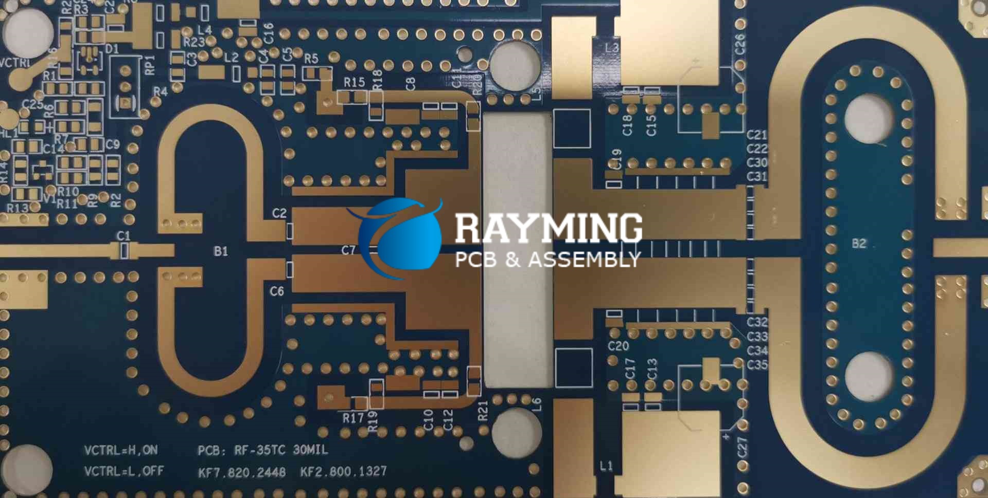
Stackup Configuration Guidelines
Rogers PCB stackups comprise alternating laminated sheets of conductor (typically rolled copper) and dielectric substrate bonded under heat and pressure. The order, thicknesses and orientations of these layers significantly impacts electrical performance.
Key stackup considerations include:
- Total layer count constraint
- Bandwidth needs dictating conductor thickness
- Stripline vs. microstrip topology
- Controlled impedance requirements
- Number of signal routing layers
- Power delivery network design
- Shielding, isolation and ventilation
Trace Geometry Guidelines
The etched copper trace geometries including width, shape and spacing determine characteristic impedance and play a major role in loss and crosstalk. Rogers provides impedance calculators and tools to derive suitable trace dimensions.
Additional trace geometry considerations:
- Match route lengths when length affects tuning
- Minimize 90 degree bends
- Employ arc, curve or mitered traces when possible
- Manage coupling and crosstalk
Fabricating Rogers Boards
Rogers PCB materials pose unique requirements throughout the fabrication process involving imaging, etching, drilling/routing, plating and solder mask steps which require special handling to prevent introducing defects or damaging the material.
Key fabrication guidelines per Rogers include:
- Ensure chemical compatibility between processes
- Adjust inner layer oxide treatment times
- Use compatible markers and rack solutions
- Optimize lamination cycles for pressure and temperature
- High helix router bits avoid fiber tearout
- Adjust hole wall preparation to ensure plating adhesion
- Watch for pink ring symptoms in drilling
- Apply finishing processes like ENIG or immersion silver
Well controlled processes tailored for microwave materials is required to achieve necessary dimensional accuracy and avoid skew or torn features.
Mitigating Thermal Issues
The moderate thermal conductivity of PTFE based materials like Rogers necessitates planning for thermal heat spreading and ventilation pathways under expected power densities to prevent hot spots which degrade electrical performance or damage components.
Common thermal management approaches include:
- Metal cored PCBs
- Embedded heat pipes or vapor chambers
- Strategic ground plane placement as heat spreaders
- Thermal vias assisting vertical conduction
- Internal layer copper fill-in to increase heat spreading
- Careful component placement avoiding hot groupings
- Selective silkscreen application if needed for ventilation
- Conformal coatings or potting compounds
Model to Measurement Correlation
Upon receiving fabbed Rogers test vehicles, measurements using vector network analyzer (VNA) test equipment should be taken on representative matched transmission lines and compared against simulations across the operating bandwidth to validate performance.
Tuning may be required if losses, reflection parameters, group delay or impedance are off expectations requiring adjustment of models before high volume fabrication.
Rogers PCB Design FAQs

What are some pros and cons of Rogers materials?
Key benefits of Rogers laminates include stable electrical performance across temperature, low loss allowing longer transmission distance and enabling high precision impedance tolerance necessary in RF designs. Drawbacks relative to FR-4 are higher cost and more fabrication process controls required.
How should signal traces be routed on outer layers for RF boards?
For best performance, critical high speed signals should use short direct path uninterrupted trace routing on outer layers rather than being split between layers. This avoids discontinuities from vias and minimizes parasitics. Right angle traces should utilize mitred bends when possible. Group aggressor signals wisely.
What special considerations exist for simulating flex PCB materials?
Analysis of flexible Rogers materials requires modeling distinct mechanical stress profiles across the anticipated dynamic bend radius and range of motion expected. This captures corresponding effects on dielectric constant and loss tangent with bending which alters electrical performance. Temperature also couples with flexure.
What tolerance is possible for Rogers controlled impedance traces?
Rogers processing allows impedance control of matched lines yielding consistency ±5% on nominal 50 ohm structures provided constraints are met during PCB layout on trace geometry, dielectric thickness and lamination pressure. Tighter tolerances are possible with advanced modeling.
How are very high speed signals routed on Rogers beyond 50 GHz?
At extreme frequencies waveguide structures replace traces, transmitting signals along micromachined channels lined with metal walls across the PCB layers. Variations guide propagation along linear or curved paths before exiting to launch onto daughterboards or antenna. Dielectrics disappear along the route. Precision microfabrication is essential.


