A rigid flex PCB (also known as rigid flexible printed circuit board) combines rigid PCBs and flexible PCB circuits together into one interconnected PCB unit. They provide solutions when dealing with complex interconnections between components in limited spaces and for applications where flexible and dynamic motion or vibration is involved.
Some key benefits of using rigid flex PCBs:
- Allows for three-dimensional design and dynamic flexing motions
- Reduced weight and space requirements
- Lower assembly costs compared to using connectors/cables
- Improved reliability with fewer interconnects
- Design freedom for product innovation
Common applications that use rigid flex PCBs:
- Consumer electronics (cellphones, laptops, wearables etc)
- Automotive electronics
- Aerospace and defense products
- Medical equipment
- Industrial robotics and machinery
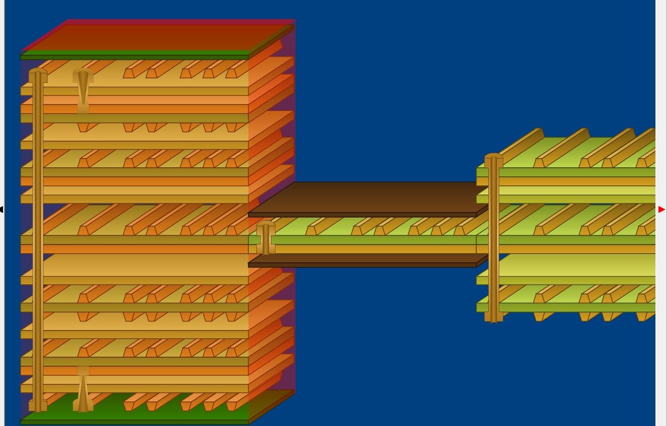
Rigid Flex PCB Stackup Design Considerations
When designing the layer stackup for a rigid flex PCB, there are several factors that need to be considered:
Layer Count
The number of conductive layers in the rigid and flex sections are usually different. Rigid sections often have higher layer counts, while flex sections usually only have 1-2 layers.
Typical rigid layer counts: 4, 6, 8 layers or more
Typical flex layer counts: 1 or 2 layers
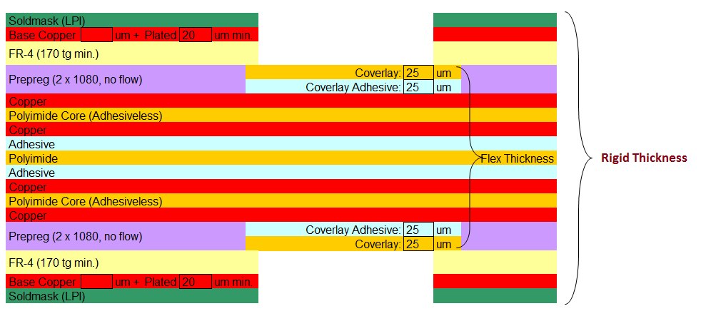
Dielectric Materials
The dielectric materials used in the rigid and flex sections also differ. Rigid sections typically use standard FR-4 dielectric. Flex sections use flexible dielectric materials such as polyimide or PTFE composites.
Copper Weight
The copper thickness also usually varies, with the rigid section having thicker copper (1oz/2oz) while the flex uses thinner copper (1/2oz or less) for flexibility.
Stiffeners
Additional stiffeners may be added to provide mechanical support and prevent warpage of the PCB during assembly and use. Common stiffener materials are aluminum, steel or FR-4.
Coverlay
An additional coverlay (protective layer) is often added to the flex sections for increased reliability and to avoid short circuits between conductors during dynamic flexing motions. Common coverlay materials include LCP, polyimide and acrylic.
Bend Radii
Appropriate bend radii need to be designed where the rigid sections transition into the flexible circuits. The bend radius affects the flex durability and dynamic fatigue life. Standard minimum bend radii recommendations should be followed.
Board Outline
The board outline design where the rigid and flex sections intersect is also important for reliability. Teardrop shapes at intersections are preferred. Avoid sharp 90 degree angles.
Rigid Flex PCB Stackup Configuration Types
There are several different rigid flex stackup configurations that can be designed:
4 Layer Rigid + 2 Layer Flex
This is the most common and cost-effective rigid flex design. It has 4 copper layers in the rigid section and 2 copper layers (top and bottom) in the flex area.
Copy code
Typical Stackup: Rigid Section: Top Solder Mask Signal Layer 1 Ground Plane Layer 2 Power Plane Layer 3 Signal Layer 4 Bottom Solder Mask Flex Section: Top Solder Mask Signal Layer 1 Signal Layer 2 Bottom Solder Mask
The ground/power planes provide controlled impedance and shielding in the rigid region. The thin 2-layer flex can flex dynamically.
6 Layer Rigid + 2 Layer Flex
This configuration increases the layer count to 6 in the rigid area while keeping the flex area as 2 layers. Allows for more signals or splitting ground/power planes.
Copy code
Typical Stackup: Rigid Section: Top Solder Mask Signal Layer 1 Ground Plane 2 Signal Layer 3 Power Plane Layer 4 Signal Layer 5 Signal Layer 6 Bottom Solder Mask Flex Section: (Unchanged) Top Solder Mask Signal Layer 1 Signal Layer 2 Bottom Solder Mask
Multi-Layer Rigid + 1 Layer Flex
Another option is to reduce the flex section down to only 1 signal layer. This provides maximum flexibility but with fewer interconnects in the dynamic section.
Copy code
Typical Stackup: Rigid Section: (6 Layer example) Top Solder Mask Signal Layer 1 Ground Plane 2 Signal Layer 3 Power Plane 4 Signal Layer 5 Signal Layer 6 Bottom Solder Mask Flex Section: Top Solder Mask Signal Layer 1 Bottom Solder Mask
Stepped Flex Layers
The number of layers in the flex section can also be gradually stepped down further away from the rigid section. This allows minimizing layers only at the most dynamic flexing areas.
Common Problems in Rigid Flex PCB Design
While rigid flex PCB technology provides many advantages, the designs can also encounter various reliability issues if not done properly. Some common rigid flex design problems include:
Pad Cratering
This refers to cracks propagating from solder pads into plated through holes causing interconnection failures. It can be prevented by proper pad shapes, annular ring sizes and reducing rigid-flex interface stresses.
Flex Cracks
Dynamic flexing motions can cause cracking of conductors or coverlay damage. Minimizing flex layers, proper bend radii, and flex materials selection lowers risks.
Via Failures
Plated through hole (PTH) vias at rigid-flex interfaces require teardrop shapes to avoid cracked connections which can cause open circuits.
Warpage
Improper lamination and/or inadequate stiffeners can lead to overall PCB warpage. This causes assembly problems and stresses interfaces leading to failures.
RF Shielding Issues
The thin flex sections often lose RF shielding capabilities in multi-layer rigid designs. This can cause signal integrity and EMI problems. Special RF gaskets or alternative shielding is needed.
Guidelines for Rigid Flex PCB Layout
Here are some key guidelines to follow when laying out the rigid flex PCB stackup in your design software:
Define Rigid-Flex Regions
Outline the exact shapes and locations of the separate rigid and flex regions as polygons. This allows applying different design rules.
Assign Dielectric Stackups
Define the different laminate materials to be used in the rigid and flex areas including dielectric constants. This ensures propersimulation.
Create Flex-Rigid Interfaces
Add rigid-flex interface lines showing the transitions between sections. This defines teardrop anchor points.
Control Impedance Changes
Mark impedance regions and define differing impedance widths on lines crossing between rigid and flex. Account for dielectric differences.
Apply Appropriate Rules
Assign specific design rules like track spacing, hole sizes, bend radii separately for the unique rigid and flex zones.
Smooth Rigid-Flex Shapes
Use teardrops, chamfers or rounded corners for all rigid-flex outline intersections to avoid stress points.
Review Layer Transitions
Clearly see how inner layer planes connect from rigid through flex sections. Check for stubs or breaks in ground/power planes.
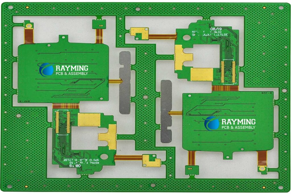
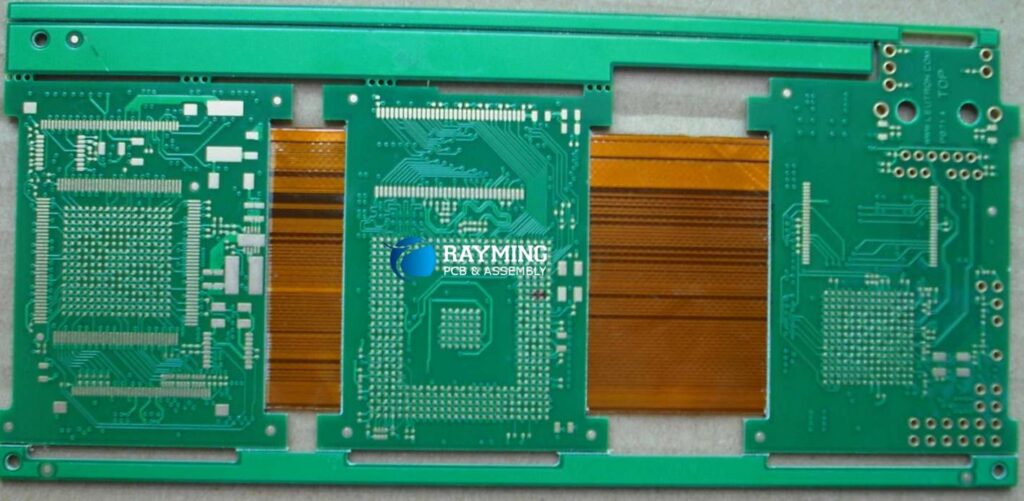
Examples of Well-Designed Rigid Flex PCBs
Here are two examples of real-world rigid flex PCBs that demonstrate good design practices:
Cell Phone Display Interconnect
- 6 layer thick rigid section for parallel high speed display signals
- 2 layer thin polyimide flex connector allows folding into compact phone enclosure
- Gradual 4 layer to 2 layer stepped rigid flex interface
- Large bend radii used on dynamic flex area
- Coverlay added for reliability enhancement
Remote Control Hobby Servo
- 4 layer standard FR-4 rigid section handles component mounting
- Single layer Kapton flex ‘tail’ allows flexible motor connections
- Sharp corners avoided at the rigid-flex junction
- Annular rings increased on pads at interfaces
- Flex section kept short and anchored for strain relief
FQA
What are the typical minimum bend radii for common flexible PCB materials?
For dynamic flexing applications, standard IPC guidelines recommend minimum bend radii of:
- Polyimide flex circuits: 10 x dielectric thickness
- PTFE composites: 12 x dielectric thickness
- LCP and PET flex: 7 x dielectric thickness
So a 3 mil thick polyimide flex, should use at least 30 mil (0.76mm) bend radius
Can components be mounted directly on both rigid and flex PCB sections?
Yes, typically components are mounted on the rigid portions of the PCB while the flex areas include only dynamic interconnections without mounted components. However, some small rigid islands can be created on the flex sections to allow mounting a few small components if required.
What are common coverlay materials used on the flexible areas of rigid flex PCBs?
Three common flexible materials used for coverlay insulation over flex circuits are:
- Liquid crystal polymer (LCP): Excellent chemical resistance and RF performance
- Polyimide: Traditional flexible insulation with good wear resistance
- Acrylic: Lower cost but provides good protection and durability
How can electrical connections be made across multiple rigid flex PCB assemblies?
For applications requiring interconnections between multiple separate rigid flex PCBs, flex-to-flex connectors can be used. These connectors have pads on the flexible tails that align precisely with pads on another rigid flex assembly for soldering or compression connections.
What are some methods used for providing RF shielding on thin flexible areas of rigid flex PCBs?
Some approaches for improving RF shielding on the thin flex regions include:
- Adhesive RF gasket material applied around flex areas
- Flex section wrapped in conductive copper tape
- Soldered or crimped metal braid around the flexible circuit regions
- Metallic enclosure brackets securing and shielding flex zones


