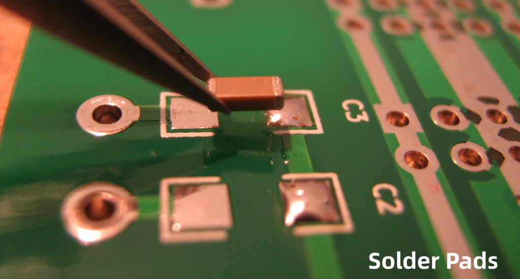
Solder pads constitute one of the most vital elements on a printed circuit board (PCB) facilitating reliable interconnections from components to copper traces during the soldering assembly process.
They represent termination points or localized metallized areas on the board providing wettable surfaces for anchoring and forming solder joints with component leads establishing both electrical continuity and mechanical anchorage.
This article provides a comprehensive perspective on various aspects related to solder pads including classifications, size calculations, spacing considerations, repair procedures and key design practices for optimal functionality.
Types of PCB Solder Pads

Based on Functionality
- Through-hole termination pads
- Surface mount pads
- Mixed solder pads
Based on Layer Position
- Top side (primary) solder pads
- Bottom side (secondary) pads
- Multi-layer pads with thermal reliefs
Other Specialized Pads
- Non-solder pads
- Testpoint probe pads
A pad’s shape and attributes get determined based on component style (through-hole vs SMD), layer of location (top or bottom side) and solderability requirements (NSMD). This enables corresponding assembly or probing needs.
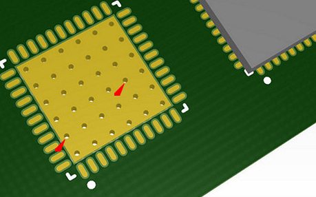
Anatomy of a Solder Pad
A solder pad features certain key elements influencing its soldering performance:
Where:
- Pad openings
- Anti-tombstoning provisions
- Solder mask web
- Copper pad area
- Non-solder coated margin
- Thermal relief spokes
Primary Areas
- Exposed pad area: Defines solderable interface
- Mask opening: Delimits solder flow areas
- NSMD margin: Prevents capillary flow escape
Secondary Aspects
- Plane spokes: Redirects heat during reflow
- Corner anchors: Check excessive solder spread
Solder Pad Design Size Calculations
Industry standards like IPC-7351 provide starting equations for estimating appropriate solder pad sizes considering component lead dimensions to meet solder joint volume needs:
Thru-Hole Pads
Pad Diameter = Lead Diameter + (2 x Annular Ring)
Annular Ring = Max(0.15mm or Lead Diameter/3, 0.25mm)
SMD Pads
Length/Width = Lead Length/Width + (2 x Toe Fillet)
Toe Fillet = Max (0.125mm or Lead Width/4, 0.25mm)
where:
- Annular Ring/Toe Fillet: Minimum contact margin
- Lead Width: Flat termination width
- Lead Length: Flat termination length
Solder Pad Spacing Considerations

In addition to adequately sized pads, sufficient clearance between adjacent pads must be provisioned to prevent solder bridging faults.
Typical Solder Pad Edge-to-Edge Spacings
| PCB Technology | Minimum Spacing | Recommended |
|---|---|---|
| Conventional SMT | 0.20mm | ≥0.25mm |
| Fine Pitch SMT | 0.15mm | ≥0.20mm |
| Ultra-Fine Pitch | 0.10mm | >0.15mm |
| High Density Interconnect | 0.075mm | >0.10mm |
Advanced CD via mask rules provide additional spacing guardbands using chamfers and expansion compensation. Minimum spacings correspond to fabrication capability while recommended values ensure assembly process coverages absorbing tolerances.
Solder Pad Repair and Modification
Defects or design revisions involving solder pads necessitate careful repair procedures without causing collateral damage. This requires:
Damage Assessment
Inspect type and extent of pad faults – nicks, inadequate sizes, spacing gaps etc. Electrically test interconnections.
Layer Access
Remove conformal coatings or components masking damaged pads requiring recovery.
Cleaning
Throughly clean resin or solder residue around pad areas taking anti-static precautions.
Build-up Metallization
Use copper adhesive foil with conductive glue or plate additional copper restoring damaged pads. May need EP/UV masking.
Insulation & Trimming
Apply solder mask or small polyimide tape strips to recreate NSMD areas or electrical spacing. Cutoversized areas.
Functionality Testing
Repeat electrical validation and visual inspection under magnification to verify successful restorations without any secondary defects before reassembly.
For extensive pad repairs especially on internal layers, alternate board replacements prove more cost-effective.
Key Solder Pad Design Practices
Adhering to certain design principles while laying out component pads ensures solder joint robustness:
1. Follow Standards
Use validated pad style, size and clearance equations from IPC-7351 as starting point. Customize if needed based on large components, higher temperatures or environmental demands.
2. Symmetry Over Shapes
Aim for uniform pad shapes on both sides oriented alike rather than mirroring complex patterns. Aids wave solderability or clamping stability.
3. Anti-Tombstoning Measures
Anchor tall components using additional pads, adhesive or deliberately asymmetric footprints countering board separation twisting moments.
4. NSMD Configurations
Extend mask web slightly past pad edges to constrain solder buildup preventing electrical shorts for tight pitches.
5. Thermal Relief Integration
Use spokes or landing area voids to redirect heat from planes preventing thermal stresses especially for large metallic pads.
6. Probe Access
Keep testpoints unmasked with adjacent spacings for reliable probing connectivity needed during diagnostics.
7. Non-Solder Finish
Specify nickel-palladium alloy finish on probe pads inhibiting solder leaching for reliable contact interface over extended test cycles.
FAQs
Can solder mask scratches near pads be repaired?
Shallow solder mask scuffs compromising spacing insulating can be recovered by spot liquid photoimageable (LPI) touchup. Ensure complete localized cure and electrical verification before assembly.
How to change solder pad sizes?
Minor pad resizing keeps same nominal footprint but alters LPI mask opening areas. For drastic dimensional changes, replace footprint and route connecting traces appropriately.
What paste voiding risks exist on solder pads?
Plane layer voids under pads cause paste sink-in rather than getting transferred onto leads. Use thicker pastes, sufficient stencil wiping during printing and baking boards prior to soldering to minimize voiding risks.
How to reduce tombstoning defects?
Strategies include anchoring opposite pad corners, extending pads further under body, using tacky solder pastes, reducing paste volumes, profiling reflow thermal ramps at moderate rates and securing tall components using fixtures during heating.
What causes solder pads to get ripped from boards?
Excessive heating levels or prolonged soldering duration leads to intermetallic diffusion Embrittlement at pad interfaces causing their lift off from boards. SMA actuated hot gas methods help overcome this over localized areas.
In summary, designing components pads by prudently considering key parameters regarding footprints, spacing, solder masking and planarity enables fabricating robust interconnections that withstand assembly and service stresses – thereby securing overall PCB reliability.


