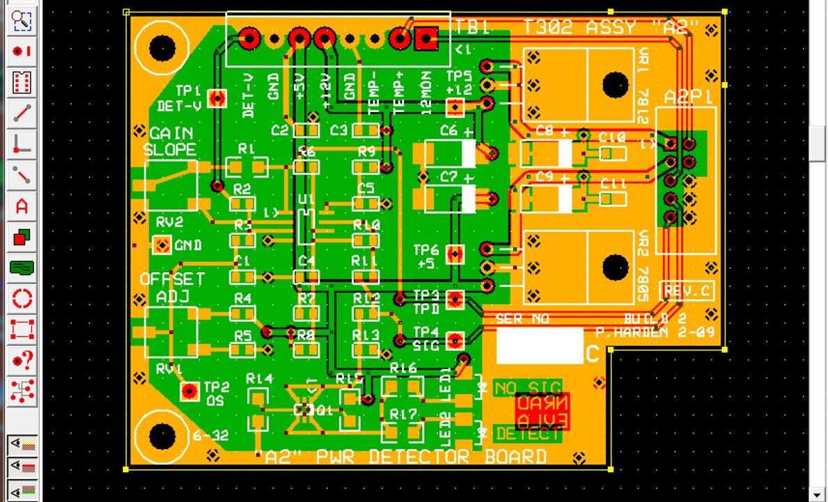
A printed circuit board (PCB) serves as the physical platform that electronically connects components using copper traces etched from laminated sheets. The PCB Layout is designed based on the electrical connectivity described in the schematic diagram.
This guide covers the following aspects involved in transforming a schematic into the corresponding PCB layout:
- Moving from schematic capture to PCB layout tools
- Setting up design constraints and planning layout
- Placement of components on board
- Routing traces to connect pads
- Finalizing layer stackup and outputs
By the end, you should have a basic methodology to take an electronic circuit schematic and convert it into a routable PCB layout file including layer plans ready for fabrication.
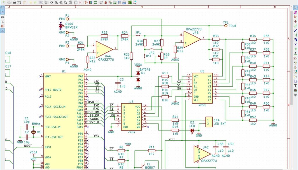
From Schematic Capture to PCB Layout
The typical electronics design flow involves:
- Creating schematic diagram in EDA tools like Altium, Eagle, KiCad etc.
- Synthesizing the schematic data into netlist files
- Importing netlist into Physical Layout tools
- Planning and placing board components
- Routing copper traces to achieve connectivity
- Documentation and manufacturing outputs
So the transition point is the netlist file generated by the EDA tool that essentially enumerates the electrical connectivity data including:
- Components used along with their attributes – names, footprints, packages etc.
- Instance identifiers e.g. IC1, Q1 to denote specific placement
- Connections through Nodes and Pins to represent nets
- Attributes like signal types or bus formations
This netlist when imported into layout software provides the starting point for planning and routing the board.
Now let us see the typical workflow steps involved in crafting the PCB layout.
Setting Up Design Rules and Constraints
Before proceeding with layout placement and routing, it is vital to configure the design rule checks and electrical constraints that would govern the PCB Fabrication and Assembly.
Key parameters include:
A. Electrical Design Rules
| Parameter | Purpose |
|---|---|
| Minimum Trace Width | Ensures adequate copper thickness to carry specified current |
| Maximum Current | Checks against excess current density as per conductor thickness |
| Impedance Control | Defines impedance tolerance limits for controlled impedance lines |
B. Physical Design Rules
| Parameter | Purpose |
|---|---|
| Minimum Hole size | Determined by smallest component lead diameter needing solderability |
| Track Spacing | Safe separation distance between adjacent copper tracks to prevent short circuits |
| Component Spacing | Minimum clearance required between adjacent components for assembly considerations |
C. Stackup Definition
| Parameter | Purpose |
|---|---|
| Layers Count | Number of conductive layers defining PCB structure and embedding possibilities for component pads and routing |
| Layer Type | Conductor vs dielectric films along with respective weights (thickness) mentioned |
| Finish | Surface plating e.g. immersion silver, OSP etc. dictated both by soldering and corrosion considerations |
| Mask Over Bare Copper | Solder resist layer type and openings |
D. Manufacturing Capabilities
| Parameter | Purpose |
|---|---|
| Minimum hole plating size | Limitation of copper plating aspect ratio through hole walls |
| Minimum track/gap | Resolution of conductors and spaces by fabrication process |
| Panel sizes | Dimensions of panel frames PCB would accommodate post breakout |
These collectively help define the constraints or the design rules within which the layout software shall operate to offer compatible outputs.
Planning Component Placement
Armed with the netlist and layout rules, next step is general placement planning even before dropping components on board including:
- Decoupling Capacitors: Place physically close to power pins of ICs
- Grouping: Logical clustering of related circuits helps organize layout
- Partitioning: High speed and noise sensitive analog away from digital/switching sections
- Power devices: Ensure easy accessibility and cooling e.g. connectors, regulators etc.
- High density regions: SMD components may have routing challenges
- Form factor constraints: Account for mounting holes, access doors, connectors etc.
- Test points: Identify signals needing probes/interfaces
- Board breakout: Plan panel utilization including rail cutting matrix
This provides a template guiding subsequent placement and routing activities.
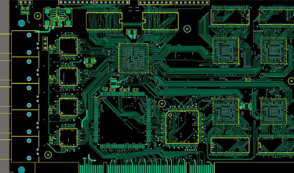
Placing Components on PCB Area
With the constraints setup and basic placement plan in place, we can start allocating components across the usable PCB space:
Some placement guidelines:
- Start with highest pin count devices first like microcontrollers, FPGAs etc.
- Allocate space for peripheral ICs, regulators around core component
- Double check pin numbers match corresponding schematic symbols during placement
- Leave adequate clearance between adjacent components as per table above
- Place interdependent sub-circuits together instead of randomly scattering
- Ensure all devices fit within the allowable canvas area
This initial component population forms the starting point for connecting them together through copper trace routing.
Routing Traces on PCB Layers
With components dropped on canvas, we can associate their pads and route physical connections between them on appropriate layers:
Some key routing considerations:
- Handle highest speed or priority nets first
- Connect ground pins directly to ground plane using vias
- Minimize via counts through optimized wire routing
- Enable visibility of all layers to visually debug alignment
- Route nets based on load currents and applicable track widths
- Use curved traces meeting adjacent pads at 900 to account for fabrication tolerance
- Space parallel traces adequately to prevent coupling
- Add test points to break long tracings into measurable sections
Through gradual connections of nodes, we can achieve a fully routed board translating schematic connectivity through layout traces.
Finalizing PCB Stackup
Based on the placement and routing complexity along with EMI and noise considerations, finalize layer types and quantities:
Examples of some popular stackups:
2 Layer Boards:
- Economical option for simple, low frequency analog or digital boards
- Top and bottom layer used for routing signals and traces
4 Layer Boards:
- Most common stackup with ground and power plane layers sandwiching top and bottom layers
- Shielded environment and availability of planes aids complex routing
6+ Layer Boards:
- Used in case of fine pitch ICs requiring large number of lanes connectivity
- Availability of multiple layers allows complex routing like DDR traces
Note: Along with layer types, also assign appropriate copper weights or dielectric film thickness as applicable.
Outputs and Documentation
Upon finalizing layout, generate industry standard outputs for design data handoff and documentation:
- Gerber Files: Layer wise plots as per fabrication shop requirements + drill file
- ODB++ Files: Standard extended output containing all netlist, layer and attributes information
- Drawings: PDF or PNG plots showing top level visual placement diagrams without actual routing
- 3D Step Model: Photorealistic 3D model showing components placement and connectors
- Bill of Materials: Listing showing all components, footprints/packages, quantities used and attributes
- Netlist: Electrical connectivity list mapped from schematic entry
These outputs allow seamless transition from design stage towards fabrication and assembly release reducing errors.
Conclusion
We have covered typical workflow followed during PCB layout design phase to transform schematic capture into routed board drawings leveraging:
- EDA software for schematic entry and netlist generation
- Constraints definition guiding electrical and layout rules
- Component placement and routing techniques
- Stackup and layer planning
- Documentation and handoff
With this end to end understanding across tools,the methodology can serve as a handy reference during your next board layout project.
Frequently Asked Questions
Q1. What is the difference between schematic and PCB Layout?
A schematic uses symbols and lines to graphically represent electronic component connectivity forming a functional circuit diagram. The PCB layout translates the schematic into actual pad locations, footprints and routed copper traces etched on a stacked board.
Q2. How to transfer schematic into PCB layout tool?
The EDA tools provide an option to generate netlist files containing components connectivity information that gets imported into layout packages. This initialization helps bringing in nets/pins data to enable board planning and tracing.
Q3. What are the typical challenges faced in converting schematics to PCBs?
Some common pain points include – tracing high speed signals without introducing distortions, achieving impedance control across interfaces, thermal management of boards with mixed analog/digital content, panel utilization optimization and dealing with large pin count fine pitch packages.
Q4. How does complexity increase from 2 layer to 6 layer PCBs?
With higher layer boards, considerable amount of pre-layout effort goes towards planning layer usage taking into account signal integrity, EMI containment, power schemes. Also exposure limitation calls for precise 3D modeling of traces to prevent short circuits during fabrication.
Q5. What role do design constraints play in PCB layout?
The design rule checks and electrical constraints predefined based on fabrication shop capabilities govern track width/spacing adherence and signal quality standards that the layout software keeps validating in background during trace routing. This ensures manufacturable data handoff.


