Vias and pads are essential features on printed circuit boards that enable routing connections between layers and mounting components. Vias connect between layers, while pads provide the bonding surfaces for attaching component terminations.
At times, pads may need to incorporate vias within them to transfer signals to other layers. But is this practice of putting vias inside pads recommended? This article explores the approach of integrating vias into pads, analyzing the tradeoffs, guidelines, limitations and effects on manufacturability and reliability.
Definitions and Basics
Before analyzing vias in pads, let’s define some key terms:
Pad: The copper surface on a PCB layer where component leads are soldered or otherwise connected. Pads allow transitioning from on-board traces to component terminations. Different pad shapes exist like round, rectangular, rounded rectangle etc.
Via: Plated through holes that provide electrical connectivity between different layers in the PCB. Signal paths transition between layers through vias. Common via types are through hole vias (PTH), blind and buried vias.
Annular Ring: The ring-shaped copper pad area surrounding the drilled hole of a plated through via. Its width must exceed minimum values for reliable plating adhesion.
Anti-Pad: Clearance area around a via where copper is removed from layers not connected by the via. Provides isolation from nearby copper.
Now, vias are sometimes embedded into component pads rather than being separate entities. Why would this be done?
Reasons to Use Vias-in-Pads

There are several motivations for integrating vias into pads:
High Density Routing – Removing anti-pad clearances between vias and pads increases routing density. Vias can be packed more closely without pad separation constraints.
Reduce Layer Transitions – A pad via transitions the signal directly from the pad to an inner layer. Without it, multiple vias would be needed – pad to outer layer and then to inner layer.
Simplify Panelization – Placing vias in the shared tooling hole pads of assembly panels avoids needing additional free vias.
Thermal Relief to Planes – A thermal spoke can connect a pad via to a ground/power plane instead of a solid direct connection for better soldering.
Lower Impedances – The parasitic inductance of pad vias is lower than routing through traces or multiple standard vias.
Lower Costs – Eliminating anti-pads and extra vias reduces fabrication costs slightly.
So in dense, high performance PCBs, embedding vias into pads provides advantages despite introducing additional considerations.
Challenges of Vias in Pads
However, integrating vias in pads also poses some challenges:
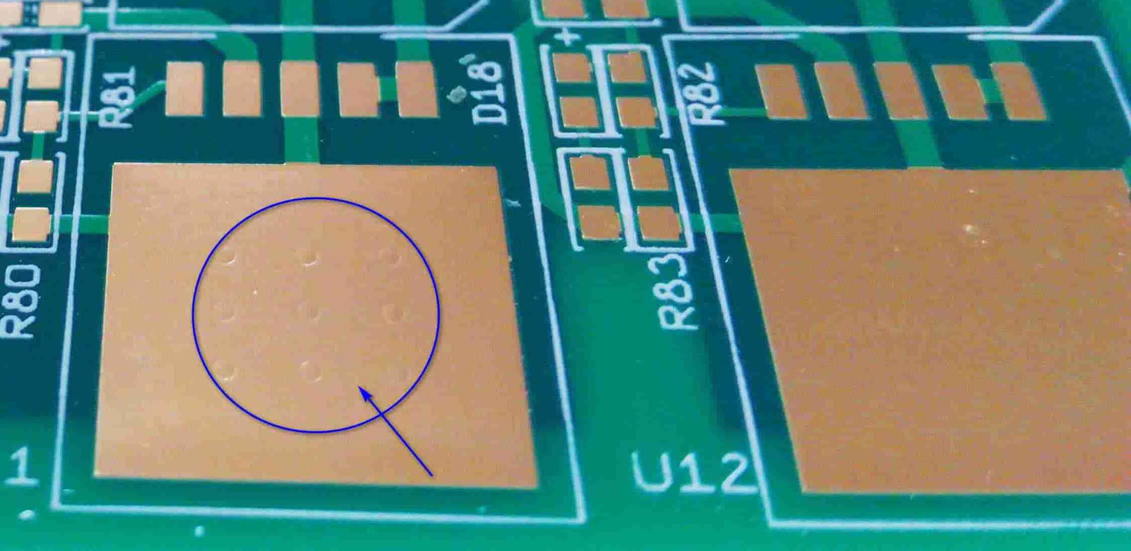
Reduced Area for Soldering – The via hole reduces the contact area between the pad and lead, which could compromise solder joint integrity.
Off-Center Pads – The via may displace the pad away from the ideal component lead location, complicating centering during assembly. Non-symmetric thermals can help counteract.
Plating Reliability – Plating adhesion could be weaker around pad via barrels compared to standard vias with full anti-pad regions.
Outgassing – Air trapped in the via hole under a lead could be problematic for BGAs during reflow with via-in-pad. Difficult to inspect also.
EMI Emissions – Gaps around leads over pad vias may cause unwanted slot antenna emissions. Specific lead-in designs help suppress.
Tombstoning – The asymmetric via location inside pads can potentially contribute to tombstoning during reflow.
With careful analysis and mitigations during design, these reliability risks can be minimized.
Manufacturing and Reliability Guidelines

Several best practices help implement vias in pads effectively:
- Maximize the annular ring width between the pad via barrel and soldering area. At least 150 microns is recommended for reliable plating.
- Use solder mask defined or non-solder mask defined pads based on the need for small vias or maximum barrel wall exposure.
- Ensure the drill diameter matches the finished via size specified. Lasers allow more precision than mechanical drilling.
- Optimize pad and anti-pad sizes together – larger anti-pads enable smaller pads for a given via size without compromising the barrel annular ring width.
- Place vias symmetrically in rectangular pads to balance thermals. Off-center locations can be used in larger circular pads.
- Specify plating copper thickness greater than 25 microns. Electroless nickel immersion gold (ENIG) plating also provides excellent pad via reliability.
- Use intermediate connections to planes/pours rather than direct connections to reduce thermal stresses.
- Perform extensive inspection and x-ray evaluation to confirm plating quality inside pad vias before assembly. Rework any under-plated holes.
- Match board and package coefficients of thermal expansion (CTE) to minimize thermal cycling strains on pad via joints.
By applying these guidelines, reliable pad vias can be implemented successfully.
Effect on Signal Integrity
In high speed designs, pad vias impact signal integrity in a few ways:
Added Capacitance – The broad copper area of the pad and via barrel introduces additional capacitive loading, slowing edge rates. Models should account for total via+pad capacitance.
Inductance Changes – Pad vias have different loop inductance versus standard vias with anti-pads. This affects impedance tuning.
Reflections – The impedance discontinuity can cause reflections of high speed signals. However, PCB traces often have more significant linewidth changes.
Resonance – The structure can resonate based on the composite pad-via inductance and capacitance. Certain high frequency signals could excite resonance.
Cross-Talk – Nearby pad vias can couple signals through electric and magnetic fields. Tight spacing needs careful evaluation.
With thoughtful high-speed design, simulation and layout strategies, pad vias can be applied successfully at multi-gigabit data rates.
Implementation Factors
Here are some considerations when applying vias in pads in PCB designs:
Via Size – Balance drill precision against reducing pad soldering area too much. Lasers allow smaller diameters than drills.
Component Type – More suitable for large BGAs vs fine pitch devices. Avoid for gullwing leads.
Pad Design – Symmetry improves reliability. Allow sufficient annular ring width.
Plane Strategy – Use intermediate pads and thermal spokes instead of connecting vias directly to planes.
Layer Planning – Determine whether pad vias are required to route escape paths.
Panel Design – Plan pad vias in tooling/indexing holes to avoid consuming free vias.
Board Density – Weigh gains in routing density against increased manufacturing risks.
Board Fabricator – Select vendors capable of producing and inspecting pad vias reliably.
Evaluating these elements early in the design process results in successful implementation.
When to Avoid Vias in Pads
Some situations where avoiding vias in pads is advised:
- Extremely dense designs with minimal clearance around pad vias
- Very high pin-count fine-pitch components
- Plated slot-through hole type vias which cannot have anti-pad clearances
- Low capability board shops without rigorous inspection and x-ray processes
- Low layer count boards where escape routing is simpler without pad vias
- Gullwing through-hole leads which require maximum pad soldering surface
- Mission-critical boards where proven conservative practices are essential
- RF designs where impedance effects of pad vias are unacceptable
- Flexible boards where pad via stresses reduce reliability during bending
The downsides can be avoided by using standard vias and improving routing channel utilization in these cases.
Example Applications Benefiting from Pad Vias

Some common situations where placing vias in pads provides advantages:
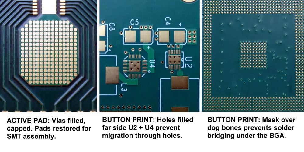
BGA Fanout – Eliminates the dogbone fanout traces required when anti-pads displace vias from pads. Simplifies dense escape routing.
Feedthroughs – A power or ground pad via can feed through a board section while allowing component attachment.
Power Distribution – Vias can splice middle layers into pad power pins allowing parallel vertical segmentation of the power net.
Signal Layer Transition – Drops high speed signals immediately to a buried layer through pad via instead of escape routing first.
Teardrop Mitigation – On outer rows, pad vias avoid the long neck teardrop traces required between pad and via.
Panelization – Shared tooling holes can incorporate vias to route their electrical connections instead of consuming free board via counts.
The applications leveraging pad vias typically involve routing complexity, density or performance challenges.
Pros and Cons Summary
Advantages of Vias-in-Pads:
- Increased routing density
- Simplify layer transitions
- Lower impedances in some configurations
- Avoid consuming separate vias
- Reduce anti-pad clearance constraints
Disadvantages of Vias-in-Pads:
- Reduced soldering pad area
- More difficult assembly centering
- Potential plating and outgassing issues
- Higher capacitance for high-speed signals
- More modeling and analysis required
By assessing the tradeoffs, designers can determine where integrating vias into pads provides sufficient benefits versus implementing standard discrete vias and pads and improving the routing channel utilization.
Conclusion
Integrating vias into the copper pads where component leads are soldered provides certain advantages in dense, high-performance PCB designs by enabling closer spacing, direct layer transitions and lower parasitic inductance. However, the reliability risks from reduced soldering area, plating concerns, precision assembly and outgassing must be mitigated through careful design, modeling and manufacturing practices. When thoughtfully architected, vias in pads can help push PCB capabilities further in next-generation electronics. But more traditional discrete via and pad arrangements still suffice for many applications where the additional considerations are unwarranted. Ultimately, the decision rests on evaluating the tradeoffs for the particular design needs at hand.
Frequently Asked Questions
Are vias required to be centered in pads?
It is not mandatory to center vias in pads, but symmetric placement balances thermals during reflow for the most reliable solder joints. In larger pads, vias can be offset if sufficient annular ring margins are maintained.
Can vias be placed in testpoint or probe pads?
Testpoint pads usually require maximum solderable surface area for probing contacts. Vias should be avoided in dedicated testpoint pads, but could be accommodated in shared functional+testpoint pads with sufficient pad area margins.
How does backdrilling affect pad vias?
When stubs are backdrilled, it creates a similar barrel hole structure as a pad via. The concepts for adequate plating, centering in pad etc. equally apply for reliable backdrilling across pad vias.
Are filled and capped vias preferred for vias in pads?
Plugging via holes does help mitigate outgassing and plating concerns. However, filled and capped vias have limited adoption due to cost and process complexity. Many designs use standard uncapped pad vias successfully.
How does solder masking affect pad via reliability?
Defaulting to solder mask defined pads provides maximum barrel wall area for plating. But non-solder mask defined pads can be used if adequate anti-pad enlargements maintain annular ring width.


