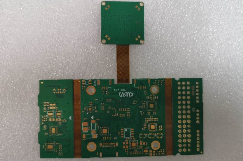
Rigid flex PCBs rigid flex pcb design guidelines combine rigid printed circuit boards and flexible printed circuit boards into a single interconnected assembly. By incorporating both rigid sections and flexible folds, rigid flex allows conformal adaptation to space constrained 3D enclosures found in products like foldable mobile devices, wearables, medical equipment, defense systems and more.
However, to reap benefits of this approach, product designers need upfront understanding of rigid flex PCB guidelines and manufacturing capabilities starting right from conceptual stages through validation to ensure reliable functioning.
This article provides a comprehensive set of considerations and best practices when adopting rigid flex PCB technology covering – architecture alternatives, layout preparations, DFA recommendations, assembly process compatibility plus testing strategies from simple to complex implementations.
Rigid Flex PCB Architecture Types
There are three fundamental rigid flex architecture configuration types provided by PCB manufacturers:
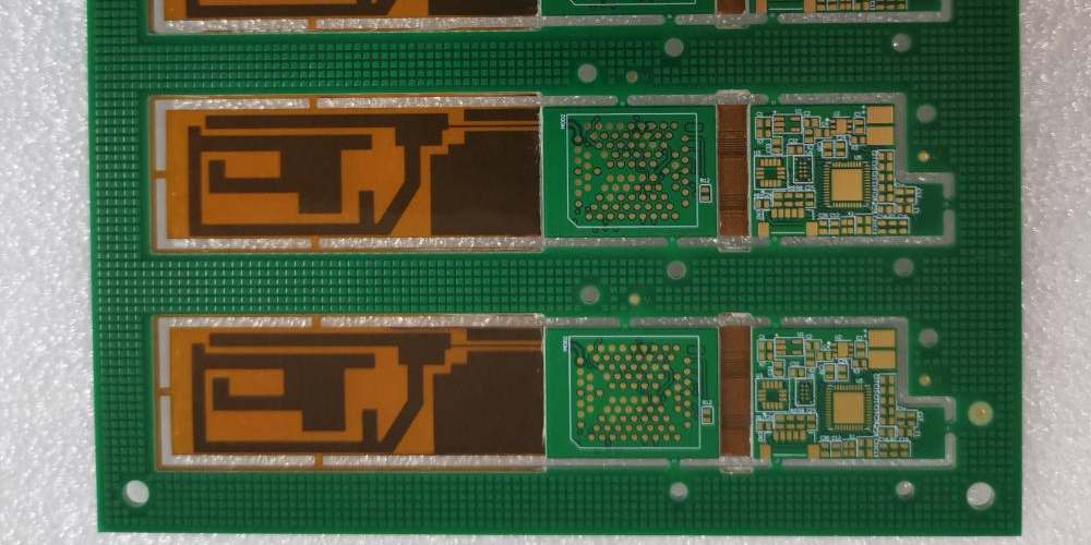
1. Flex-Rigid PCBs
These contain multiple discreet rigid PCBs interconnected by flexible circuits. Allows encapsulated rigid sections optimized for component placement/routing to be joined by dynamic folds.
2. Rigid-Flex PCBs
This architecture has main baseline rigid PCB region with extended flexible tongues protruding externally. Allows static rigid zone for core electronics while having dynamic external connections.
3. Complex Rigid-Flex PCBs
Advanced configurations contain both rigid sections and complex multiple flex layers in sandwich arrangement allowing routing across layers. Used in highly integrated electromechanical products needing system optimization.
For each type, designers must translate end product requirements into implementation guidelines that fabrication/assembly houses can successfully manufacture with quality, reliability and cost considerations factored in.
Rigid Flex Design Guidelines
Following are key rigid flex design checklist applicable across above architectural styles from simple to complex implementations:
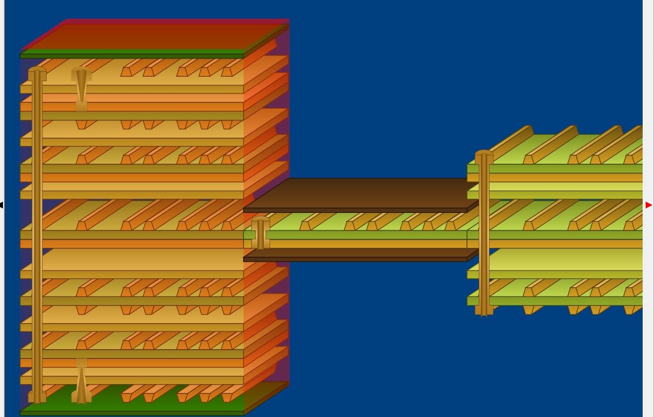
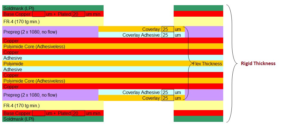
1. Layer Stack Planning
- Define rigid layer counts needed for component densities plus signal routing paths
- Specify flexible stackup including single/double sided sections based on complexity
- Select dielectrics like polyimide for layers allowing flex folding without cracking
- Indicate cutouts, cavities required in rigid areas for placement or space savings
2. Specify Flex Layer Parameters
- Indicate static and dynamic flex zones in design files
- Mark minimum bend radius constraints for dynamic regions per flex thickness
- Highlight orientation of bends: inwards or outwards based on assembly steps
- Define Keepout zones preventing components/traces in flex bending areas
3. Electrical Rules Implementation
- Set trace widths/spacings as per current needs with thicker copper for high current power lines
- Specify impedance rules critical for high speed interfaces eye diagrams
- Define ground stitching vias separating analog and digital logic preventing noise coupling
- Implement power decoupling capacitors near IC pads minimizing ripples
4. Stackup and Copper Balancing
- Ensure copper thickness balanced on both sides of flexible layers
- Symmetric rigid layer planning either side of embedded passives/actives for stability
- Equal area copper fills on each layer to prevent warpage under temperature excursions
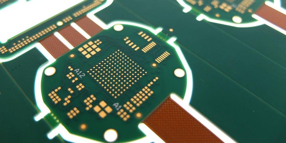
5. Component Selection and Placement
- Select surface mount components compatible with reflow soldering process where possible
- Specify flexible adhesive choices like anisotropic conductive films based on fine pad pitch sizes
- Define no-clean flux protocols amenable for washing if needed for residue prevention during complex assembly steps
6. Board Outline and Tooling
- Specify board profile contours aligned to assembly fixtures
- Define locations of jigs/handling points easing complex assembly
- Indicate locations for testpoints accessible during manufacturing process steps
- Provide mounting points and keepouts for structural reinforcements like stiffeners
7. Panel Utilization Optimization
- Layout individual PCBs targeting high utilization/yield per panel based on board shop capability
- Array components targeting minimizing routing congestion proximate to dicing channels
- Implement breakaway tabs, test coupons assisting post-production panelization steps
Above guidelines instituted up front using constraints management in layout tools smooths manufacturing handoff reducing cost surprises and delays down the line due to re-spins. We next highlight some special considerations when dealing with conventional SMT lines versus advanced packaging equipment.
SMT Assembly Rules for Rigid Flex PCBs
Use of standardized SMT lines for assembly provides a low cost advantage. Designers must collaborate with assembly partners early to define process capability and accordingly set implementation rules:
1. Component Types: Stay compliant with industry standard chip package footprints and shapes for reliable placement, solder paste deposition and post reflow quality checks. Confirm compatibility of BGAs, QFPs, 01005 chip components etc.
2. Fine Pitch Components: Understand allowable component miniaturization limits based on SMT line’s precision plus implement adhesive alternatives like conductive epoxies matching small pad geometries. This smoothes small pitch BGAs, CSPs and 01005 LED handling.
3. Flex Fold Limitations: Determine allowable dimensions for rigid islands based on standard conveyor widths through SMT oven, chip shooter, X-ray plus visual inspection stations. Go beyond limits only if custom carriers are viable.
4. Panel Sizes: Target panel dimensions which are optimally handled by SMT feeders, panel turner mechanisms etc through different process steps without need for specialist operations. Typical max limit is 18″x24″ for medium volume lines.
5. Test Access: Ensure testpoints on boards are SMT mountable for interfacing with test-fixtures used for In-Circuit-Testers plus functional validation yielding go/no-go feedback.
Upfront dialogue with assembly partners steers designers clear of potential process snags when leveraging standard SMT lines for cost sensitive builds.
Guidelines for Advanced Packaging Integration
For high complexity rigid flex implementations demanding tight feature sizes, space constraints plus assembly process intricacies like multilayer flex or embedded actives – migrating to advanced packaging production environments is recommended marrying design to capability:
1. Chip Embedding Options: Explore embedding bare die or fan-out wafer level packaging underneath flex/rigid layers unlocking space savings versus external placement. This calls for high accuracy alignment equipment.
2. Fine Lines and Spaces: Implement trace dimensions approaching 1 mil line with 1 mil spacing getting >20 traces per mm enabled by transducer based SMT pick place heads. Necessitates matching board and package footprints.
3. Miniaturized Passives Integration: Embed tiny 01005 and 008004 chip passives, capacitors, resistors within flex and rigid layers linked with stacked microvias to functionally replace larger 0402 discretes.
4. Tight Component and Layer Stacking: Stack components on both sides of thin cores routing traces through microvias in high density HDI style builds reducing layer count versus planar routing. Needs advanced DFM feedback.
5. Advanced Materials: Move beyond standard FR-4 rigid cores to high speed dielectrics like Polyimide, PTFE reducing signal loss. Further integrate exotic heat sink materials for thermal management of embedded actives.
While transitioning to advanced packaging calls for upfront equipment and process understanding – it opens the gateway for product miniaturization beyond constraints of conventional PCB metrics into domain of electronic manufacturing systems.
Rigid Flex PCB Design for Assembly Guidelines
To ensure manufacturability and operational reliability of rigid flex PCBs – designers need to analyze assembly steps beyond just fabrication design rules compliance touching on production constraints too:
1. Layer Transitions: Define minimum spacing between successive layer transitions on a design to allow machining of slots, cavities etc without impacting features on layers above or below through the stackup.
2. Fiducials: Embed board assembly fiducials referencing the product enclosure and housing features allowing precise vision inspection guided alignment during placement of components in respective zones.
3. Stiffener Integration: Incorporate global or sectional stiffeners within rigid portions adjacent to dynamic folds using analysis feedback preventing undue flexing during product lifetime.
4. Shielding: Implement fine mesh EMI shielding on flex mid plane referencing ground for shielding effect. Alternatively, plan for enclosure based shielding Mechanism attachment features around openings.
5. Thermal Pads: Incorporate bottom side thermal pads in the rigid portion for interfacing with external heat sinks pulling heat away from embedded/surface mount components.
6. Test Points: Define probe test points on product to enable in circuit testing at sub assembly levels through the complex build sequence when full product assembly still incomplete. Enables early validation.
Above considerations bridging across logical design requirements, assembly process capabilities and inspection/test needs representative of the production environment constraints allows fabrication release success.
Rigid Flex PCB Design Validation
To prevent late stage design churn impacting cost/schedule – upfront modeling analysis providing predictive performance feedback combined with risk mitigation steps allows design validation:
1. Layer Stack Modeling: Use impedance calculators and 2D field solvers to model selected stackup measuring single ended impedance, coupled noise between traces and reference planes indicating tuning needs meeting speed requirements.
2. Dynamic Fold Analysis: Leverage FEA solvers to simulate lifespan bending cycles at flex fold regions – assessing strain levels on traces confirming reliability over service loads avoiding early field failures.
3. Thermal Modeling: Perform thermal simulation on most heated zones under max load conditions – ensuring components work within safe case and junction temperature range through entire operating envelope through sufficient cooling or heat sinking.
4. EMI Analysis: Execute 3D EM simulations on chosen multi-layer stackup models excited by edge launch and surface mount antennas. Use results to refine shielding, enclosure treatments plus IO line filtering required to meet EMC emissions limits.
5. Prototype Test: Validate designs with test vehicle builds through accelerated stress testing including dynamic bend cycles, humidity/temperature soaks plus vibration exposure before committing to pilot runs.
Above modeling analyses provides insights to make optimal balancing decisions across performance, reliability and cost helping achieve volume production success for rigid flex PCB projects – avoiding unbudgeted spins due to late validation.
Summary of Rigid Flex Design Best Practices
Below key guidelines checklist summarizes rigid flex PCB optimization steps for manufacturability and operational reliability:
- Simulate signal, power, environmental integrity with modeling feedback
- Set constraints for geometry, spacing driven by process capabilities
- Assess thermal loads, EMI risks early through desk analysis
- Define testpoints upfront aiding validation during assembly
- Dialogue with fab/assembly shop on DFx optimizations
- Build in design margin balancing performance versus cost
With increasing need for compact, customized solutions – rigid flex PCBs serve an enabling role marrying electrical functionality into tailored form factors meeting exacting environmental resilience requirements.
Getting the design principles right through a structured development flow is key to reaping benefits from this technology while de-risking manufacturing handoff leading to operational field success.
Frequently Asked Questions
Q1. What are key benefits of a rigid flex PCB?
Rigid flex PCB technology allows embedding electrical functionality into ergonomic and space saving forms ideal for product miniaturization and portability requirements demanded by consumer and industrial markets.
Q2. What analysis validates performance of rigid flex designs?
Modeling using finite element method and 3D EM solvers on proposed rigid flex board geometries allows simulation of operational stresses enabling integrity confirmation and design hardening before committing to production.
Q3. What fabrication process makes rigid flex PCBs?
Rigid flex PCBs leverage additive print film deposition processes allowing combination of flexible polyimide films with rigid laminates to create hybrid boards then put through subtractive copper patterning by chemical milling and drilling steps building interconnects.
Q4. What design areas need special attention?
Dynamic flex fold areas in terms of bend radius rules plus balancing equal copper on both sides of flex core to ensure stability under environmental temperature condition changes need careful implementation.
Q5. How to manage product design to fab handoff?
Upfront design collateral highlighting constraints, identifying process capability needs plus dialoguing with fabrication and assembly partners through design cycle allows organization of seamless manufacturing transfer minimizing cost or schedule overruns.


