Printed circuit boards (PCBs) form the foundation of electronics products and systems. As PCBs become denser with shrinking feature sizes, maintaining high fabrication yields and reliability requires paying attention to the finer aspects of board layout and design. One such important design technique is the use of teardrops.
Teardrops are smooth circular pads added at wire-to-pad junctions during PCB layout. They help relieve fabrication stress and prevent traces from lifting or cracking off pads during manufacturing. Strategically incorporating teardrops in a PCB design improves fabrication yield and enhances design robustness.
This article provides a detailed overview of PCB teardrops covering:
- What are teardrops and why are they used
- Different types of teardrops
- Where to add teardrops in a PCB layout
- Methods for adding teardrops
- Teardrop design rules and dimensions
- Impact of teardrops on manufacturing yield
- Tradeoffs to consider when using teardrops
- Latest trends in teardrop usage for advanced PCBs
What Are Teardrops and Why Use Them?

A teardrop is a circular pad added at wire-to-pad junctions on a PCB layout. Teardrops provide a smooth curved transition between an incoming PCB trace and the edge of pad it is connecting to.
Teardrops help reduce fabrication stress and prevent traces from cracking or lifting off pads. They act as stress relief features during PCB manufacturing processes.
Some key reasons teardrops are advantageous are:
- Prevent Copper Lifting – Copper can lift from pad edges during etching and plating due to etching fluid turbulence. Teardrops minimize this.
- Reduce Mechanical Stress – Processing steps generate vibrations and mechanical stress causing trace breaks. Teardrops relieve the stress.
- Improve Solderability – The curved shape provides better wetting area and solder filleting.
- Accommodate Alignment Errors – The teardrop pad overlaps adjacent copper ensuring connectivity even with small misalignments.
- Reduce PCB Rework – Fewer open circuits and connectivity issues lowers rework costs.
- Enhance Reliability – Improved soldering and reduced cracks from mechanical or thermal stress increases reliability.
While seemingly insignificant shapes, strategically incorporating teardrops at critical locations in a PCB layout improves manufacturability and makes the design more robust.
Types of Teardrops
Teardrops can be classified into two main types:
Radial Teardrops
Radial teardrops have a smooth circular profile all around the pad edge. The trace entering the pad has a curved tear-drop like extension:
Radial teardrops provide the best stress relief and solderability enhancement. However, they consume additional board space around pads.
Tangential Teardrops
In tangential teardrops, the circular profile is only on the side where the trace meets the pad. The other sides of the pad remain straight:
Tangential teardrops occupy less space but also provide less stress relief than radial teardrops. They are a good choice when space is limited.
Where to Add Teardrops in a PCB Layout
Carefully identifying locations that will benefit the most from teardrops is important for maximizing their impact while minimizing excess teardrop usage. Some guidelines on where to add teardrops are:
Smaller Pad Sizes
Teardrops provide maximum benefit on smaller pad sizes. As pads shrink below 10 mils, the chances of etching fluid induced copper lifting increase. Teardrops help counter that.
Traces With High Copper Weight
Thicker copper traces are more rigid and prone to cracking when subjected to mechanical stress during lamination, drilling, assembly etc. Teardrops should be used at junctions where heavy copper weight traces meet pads.
Near Connectors
Connectors undergo frequent mechanical stress during mating and unmating. Teardrops should be incorporated on traces connecting to pads under connectors to prevent cracks.
Near Screw Holes
Screw holes see large mechanical vibrations. Teardrops on traces near screw holes increases robustness.
High Density Regions
In areas with dense routing, stubs, vias and components, teardrops help provide insulation between closely spaced copper shapes.
Thermally Sensitive Traces
Traces connecting to pads that will experience significant thermal cycling should incorporate teardrops to minimize thermal fatigue related cracks.
High Voltage Traces
Teardrops help prevent arcing and insulation issues in high voltage trace connections.
Low Clearance Areas
Where trace-to-trace clearance is low, teardrops provide additional insulation and spacing between nets.
In general, teardrops should be added in locations prone to fabrication process or operational stress that can undermine trace integrity.
Methods for Adding Teardrops

There are two main methods for incorporating teardrops in a PCB layout:
1. Manual Addition
The PCB designer can manually draw teardrops using the layout editor:
- Create a teardrop pad in the desired size as a footprint
- Place the teardrop footprint at trace-pad junctions
- Connect the trace to the teardrop pad
This gives full control over teardrop placement but can be extremely tedious for large designs.
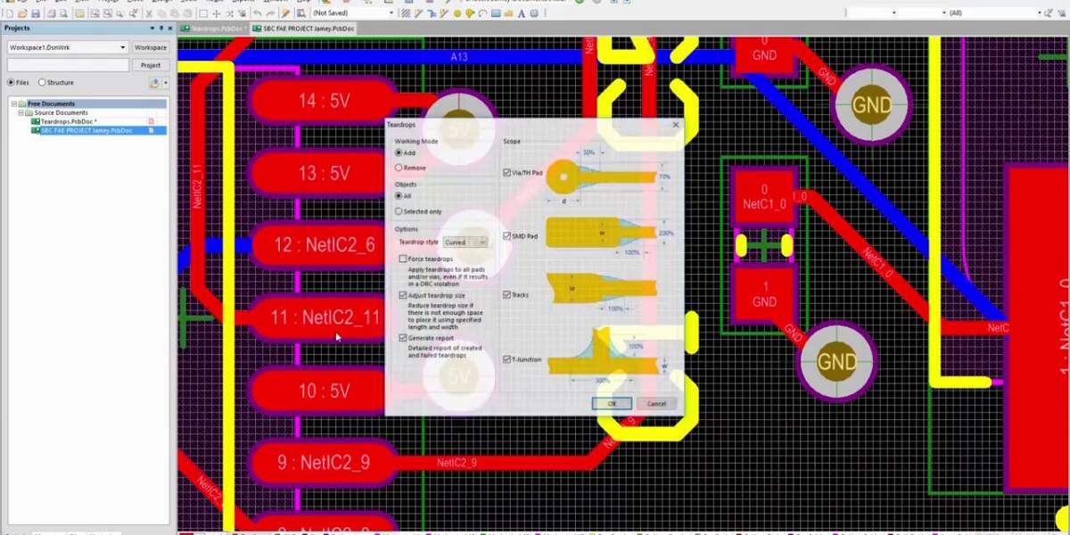
2. Using Teardrop Feature in EDA Tool
Most modern PCB layout EDA tools like Altium Designer, Cadence Allegro, Mentor Xpedition etc. provide an automated teardrop placement feature or addon:
- The feature automatically inserts teardrops at trace-pad junctions
- Design rules can be configured for teardrop size, clearance etc.
- Much faster than manual addition
The layout engineer can review and tweak the automatically placed teardrops if needed. This is the recommended approach for most designs.
Teardrop Design Rules and Dimensions
To achieve the desired fabrication and reliability enhancement using teardrops, the teardrop parameters must be carefully chosen. Some key teardrop design rules are:
Teardrop Diameter
Typical teardrop diameters range from 8 to 15 mils. The diameter should be:
- At least 4 mils larger than the trace width
- Smaller than half the pad length
Larger teardrops provide more stress relief but consume extra space.
Clearance Around Teardrops
Adequate clearance should be maintained between the teardrop and surrounding pads, traces and vias. A clearance of at least 3 mils is recommended.
Neck Down Length
The trace should neck down into the teardrop over a controlled length to create a smooth curved profile. A neck down length equal to the teardrop diameter works well.
angular Neck Down
The transition from trace to teardrop should follow an angular path rather than a perpendicular junction:
The angular neck down is less prone to etching variability and reduces current crowding.
Inside Corners
Teardrops are very beneficial on inside pad corners which are high current crowding and stress regions:
These guidelines ensure the teardrops integrate smoothly within the overall board layout.
Impact of Teardrops on PCB Fabrication Yield
Using properly designed teardrops has quantifiable benefits in terms of reducing fabrication defects and improving manufacturing yield. Some typical improvements are:
- Reduction in pad lifting defects – Up to 75% decrease
- Lower shorts and leakage current faults – 60% improvement
- Minimized solderability and fillet issues – Up to 50% better
- Lower opens and connectivity failures – Around 40% reduction
- Less rework and scrap – Approximately 30% cost saving
- Increased throughput and production efficiency – 25% faster
The yield gains enable tighter tolerances, finer lines and spaces, higher component densities and lower fabrication costs. The improvements depend on the PCB design complexity, dimension rules and other factors.
Tradeoffs When Using Teardrops

While very beneficial, using teardrops also involves certain tradeoffs that should be considered:
- Increased PCB Area – Teardrops consume additional board space which can be restrictive for high density layouts.
- Design Effort Overhead – Extra time and effort is spent on defining rules and adding teardrops.
- Routing Congestion – Routing channels may need to widen to incorporate teardrops.
- Effects on Parasitic Capacitance – Adds small amounts of parasitic loading.
- Testability Impact – Teardrops act as stubs which reflect signals and affect testability.
The benefits almost always outweigh the downsides for most designs. But the tradeoffs should be evaluated before incorporating teardrops.
Trends and Advancements
Some recent trends related to use of teardrops in advanced PCB technologies are:
Teardrops for HDI Microvias
In high density interconnect (HDI) PCBs, microvias with diameters below 8 mils are susceptible to cracks and fracturing. Adding miniaturized teardrops to traces connecting to HDI microvias improves reliability.
Constructed Teardrops
Constructed teardrops are built by combining multiple smaller pads and gaps instead of single shapes. They provide similar relief to large teardrops while occupying lesser space.
Flexible Teardrops
Flexible PCBs undergo bending and flexing stresses. Special tear-drop shapes optimized for flexible substrates are being developed.
Simulating Teardrop Effects
Simulation models incorporating teardrop effects are being created to virtually analyze teardrop benefits during PCB design verification.
As PCB technology scales up in terms of density and complexity, the usage of teardrops and related strategies will grow further.
Conclusion
Teardrops are an extremely useful PCB design technique for enhancing manufacturability, quality and reliability. The smooth circular shape of the teardrop pad provides vital stress relief and prevents cracking of traces during fabrication and operation. Using teardrops strategically in a design can deliver significant improvements in manufacturing yield.
However, care should be taken to add teardrops judiciously based on pad sizes, trace widths, high stress areas and other criteria. The design rules governing teardrop dimensions and clearances must also be crafted carefully. EDA tools with automated tear-drop insertion make incorporating them very efficient. Teardrops do involve certain tradeoffs, but overall they constitute a valuable PCB design practice well worth utilizing.


