
Introduction to PCB Development
Printed circuit boards (PCBs) are an essential component of electronic devices. They provide the foundation for mounting and interconnecting electronic components. Developing a new PCB is a complex process involving many steps from initial design through to final fabrication and assembly.
This article provides a comprehensive overview of the PCB development workflow including:
- PCB design and layout
- Prototyping iterations
- Fabrication and assembly
- Testing and verification
- Documentation and data management
Understanding the process of bringing a new PCB from concept to high volume production is key for both electronics engineers and PCB supply chain partners.
PCB Design and Layout
The PCB development process starts with schematic capture and board layout. This is where the circuit structure and physical board design are created.
Schematic Capture
Schematic capture involves using ECAD software to draw the electronic schematic. This shows the components and connectivity of the circuit. Key steps in schematic capture include:
- Placing components: Add all required components from libraries into the design such as ICs, resistors, capacitors.
- Connecting components: Wire up components according to the circuit logic requirements.
- Adding power/ground: Connect components to power and ground nets.
- Adding other networks: Include any other required connectivity like high speed or differential signaling networks.
- Simulating/validating design: Perform circuit simulation and design rule checks to validate schematic integrity.
The output of schematic capture is the unrouted connectivity of the circuit. All components and logical connections are defined.
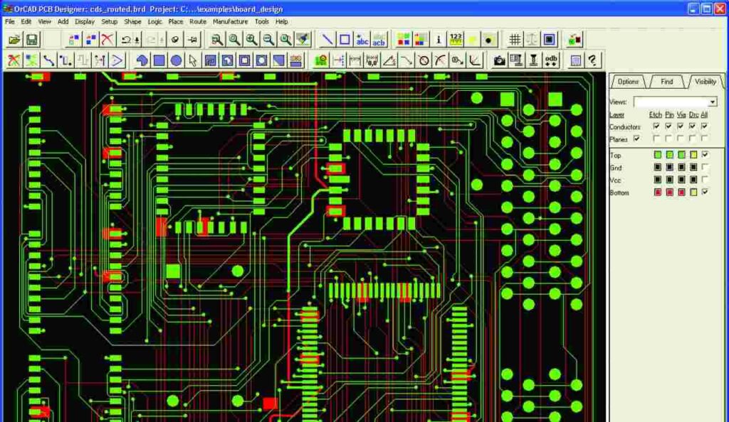
PCB Layout
With the schematic completed, the physical board layout is created. This involves:
- Placing components: Components are arranged on the board canvas according to placement rules.
- Routing connections: Wires are routed between points to form copper tracks on board layers.
- Assigning power/ground: Power and ground nets are assigned to board layers.
- Placing supporting features: Other physical design elements like cutouts, holes, silkscreen, solder masks.
- Validating design rules: Electrical and physical constraints are validated.
The designer must optimize the layout for metrics like signal integrity, component density, manufacturability. Iterating the layout is usually required to refine the design.
Output Design Data
completion of board layout, the ECAD software outputs a comprehensive set of design data including:
- Gerber files: Standard format for circuit copper layers, solder masks, silkscreen, etc.
- Drill files: Locations of holes to be drilled.
- Bill of Materials: List of components for circuit population.
- Netlist: Connectivity list for assembly.
- Mechanical drawings: 2D/3D drawings for enclosure design.
This design output package fully defines the PCB ready for fabrication and assembly.
PCB Prototyping
Before committing to full production, most PCB designs go through prototyping iterations to validate the design. This is an opportunity to:
- Confirm the circuit works as intended.
- Check PCB manufacturability.
- Refine component placement and routing.
- Optimize performance issues or errors.
Prototyping involves producing a small batch of boards for testing. After evaluation, an updated version is fabricated incorporating any learnings.
Prototype Fabrication
Prototypes are fabricated in small quantities, typically 5-10 boards. specialized prototype PCB suppliers offer fast turnaround times to enable quick design iterations.
Once the Gerber and drill files are sent to the prototype supplier, standard turnaround is 24-48 hours. More complex designs may take 3-5 days.
Assembling the Prototype
With fabricated bare boards in hand, the next step is populating the components. This can be done in-house or by utilizing an electronics manufacturing services (EMS) provider.
Key aspects of prototype assembly include:
- Sourcing components – Obtain all required ICs, passives, connectors in appropriate quantities.
- Stencil printing solder paste – Use a prototype stencil to apply paste to pads.
- Pick and place components – Use manual or automated pick-and-place system.
- Reflow soldering – Pass boards through a reflow oven melting paste to attach components.
- Inspect solder joints – Verify all components are properly soldered with quality joints.
- Functional test – Do basic power-up tests to ensure boards are functioning.
The assembled boards are now ready for comprehensive design validation testing.
Design Validation Testing
Thoroughly testing the prototype boards is critical for identifying any issues and improving the design. Typical validation testing includes:
General Functional Testing
- Power on – does the board turn on and boot up?
- Subsystem validation – check main functions are working.
- Feature validation – verify key integrated features perform properly.
Design Review
- Component placement – check spacing and rotation.
- Routing review – look for crosstalk risks or EMI concerns.
- Manufacturability – identify any assembly or test issues.
Environmental Stress Testing
- Thermal cycling – hot and cold soaks.
- Drop/shock/vibration.
- Humidity/moisture soaks.
Compliance Testing
- Safety – UL, IEC 60950.
- EMI/EMC – radiated emissions, susceptibility, surge.
Performance Optimization
- Signal integrity – minimize transmission line effects.
- EMI mitigation – reduce unwanted emissions.
- Tune power integrity – stabilize power supply noise.
By thoroughly testing the prototype, the design can be revised to address any issues prior to release for production. It is normal to build 2-3 cycles of prototypes before finalizing the design.
PCB Fabrication and Assembly
Once the design is finalized after prototype iterations, it moves to volume fabrication and assembly for production. This involves:
Fabrication Data Package
The fabrication data package provides all information needed to build the boards including:
- Gerber files for each layer
- Bill of materials listing all components
- Assembly drawings showing component placements
- Drill/rout files specifying hole locations
- IPC netlist detailing component connectivity
- Any special instructions for the fabricator
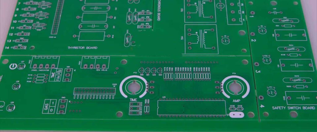
Fabrication
The fabrication facility processes the bare boards. This includes:
- CAM – Computer aided manufacturing programs are generated.
- Panelization – Individual PCB designs are arranged on large panels for mass production.
- Copper patterning – Using lithography the copper layers are imaged.
- Etching – Unwanted copper is etched away leaving the desired traces.
- Lamination – Alternating layers of dielectric prepreg and copper are pressed together and cured with heat.
- Drilling – Holes are mechanically drilled or laser drilled based on the drill file.
- Plating – Copper is plated on the interior of drilled holes and over board surfaces.
- Coating – Layers like solder mask, silkscreen, and surface finish are applied.
- Scoring/routing – Individual boards are cut from the larger panels.
- Inspection – 100% of boards are optically inspected for defects.
- Electrical test – Bare boards are electrically probed to verify connectivity.
This comprehensive fabrication process converts the original design files into completed bare PCBs ready for component assembly.
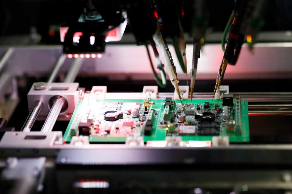
Assembly
The board assembly process attaches and interconnects components to the boards. Assembly involves:
- Solder paste application – Solder paste is printed on pads using a stencil.
- Pick and place – Robotic systems place components onto the paste-covered pads.
- Reflow soldering – The assembled board is heated in a reflow oven to form solder joints.
- Inspection – Boards are visually inspected to check placement and joint quality.
- Testing – Electrical tests validate proper assembly and function.
- Conformal coating – A protective coating may be selectively applied.
- Packaging – Boards are individually or batch packaged for shipment.
The final result is fully assembled PCBs complete with components ready for integration into electronic products.
Testing and Verification
Once assembled PCBs are received from production, comprehensive testing and verification takes place:
Incoming Quality Inspection
- Visual inspection – Check for any obvious assembly defects and workmanship issues. Verify correct components populated.
- In-circuit test – Use test probes to electrically validate correct assembly of components.
- X-ray inspection – X-ray images allow inspection of internal solder joints including hidden connections.
Quality Conformance Testing
- Functional testing – Validate core functionality and performance meet requirements.
- Environmental stress testing – Subject boards to stresses like temperature, vibration, humidity.
- HALT testing – Highly accelerated life testing identifies design weaknesses.
- Compliance testing – Confirm certification needs like FCC, CE, UL.
Reliability Demonstration
- HASS testing – Highly accelerated stress screening under thermal and vibration stresses.
- Life testing – Operate boards at specification limits for extended duration to validate reliability.
- MTBF estimation – Using part failure rates and derating conditions, estimate mean time before failure.
Thorough testing provides confidence in board quality and reliability before integration into end products. Issues identified can be referred back to fabrication or design teams.
Documentation and Data Management
Clear documentation and data management are key parts of the PCB development process:
Documentation
- Specifications – Comprehensive specifications detailing all board requirements, acceptance criteria, and quality processes.
- Assembly drawings – Illustrate component placements, markings, dimensions, and callouts.
- Schematics/block diagrams – Show circuit structure, hierarchy, interfaces, and functions.
- BOM/approved vendor lists – List exact components and approved supply chain sources.
- Test procedures/reports – Document all qualification and conformance testing performed.
- CAM instructions – Special instructions for PCB fabrication and assembly.
- Certification reports – Results and certificates from regulatory certification testing.
Data Management
- Schematic/layout source files – Original ECAD data used to design board.
- Gerber manufacturing files – Layer images data for fabrication.
- Bill of materials – Component list with approved manufacturer parts numbers.
- Assembly drawings – Mechanical drawings illustrating component placements.
- Firmware/software – Any firmware or embedded software for the product.
Keeping organized, versioned documentation and design data is crucial for understanding, replicating, and updating any electronics design over its lifecycle.
Frequently Asked Questions
Here are some common questions about PCB development processes:
What are the main steps in developing a new PCB?
The key stages are: design/layout, prototype fabrication/assembly, validation testing, volume fabrication, assembly for production, quality/reliability testing, and documentation.
What types of validation testing are done on PCB prototypes?
Typical tests include functionality, design review, environmental stress, standards compliance, and performance optimization. This comprehensive testing allows the design to be refined before production.
How long does it take to develop a new PCB?
For a typical low-to-moderate complexity board, development through prototyping may take 1-2 months. Finalizing fabrication and assembly for production could then take an additional 1-2 months. More complex designs can take significantly longer.
What data is required to fabricate and assemble PCBs?
The fabrication package includes Gerber files, drill files, BOM, assembly drawings, and CAM instructions. The assembly facility needs the bare boards, components, BOM, assembly drawings, and pick-and-place data.
How are PCB assemblies tested in production?
Incoming quality inspection checks for defects. Functional testing verifies operation. Environmental stress screening and life testing demonstrate reliability and lifetime.


