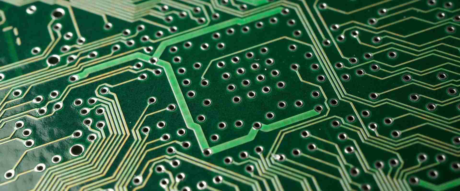
A via hole is one of the most fundamental features used in printed circuit boards (PCB) to provide electrical and mechanical connections between the copper layers. Vias enable routing traces vertically across layers, stitch power and ground planes, carry signals between layers, and facilitate component mounting and heat transfer in multilayer PCB designs.
This article will provide a detailed understanding of what vias are, their types, design considerations, how they are manufactured and key roles they serve in enabling high density interconnect PCBs.
What is a Via?
A via is a vertical plated through hole used in printed circuit boards to interconnect copper layers and provide electrical conduction between layers. It comprises the following elements:
- Hole Drilled Through PCB Layers: Cylindrical hole through some or all the layers of the PCB material.
- Metallization of Hole Walls: The inner walls of the drilled hole are plated with copper to make it electrically conductive.
- Annular Copper Ring on Layers: Annular pad around via hole on each layer for connecting traces.
- Plating Connecting Layers: Electroplated copper deposits from hole walls connect to copper on adjacent layers.
Vias provide a conductive path enabling vertical transitions and 3D routing capability in multilayer PCBs.
Why are Vias Needed in PCBs?

Vias serve several important functions that are essential for high density PCB designs:
Interlayer Connections for Traces
Vias enable routing traces between different layers of the PCB by connecting copper on adjacent layers through the plated hole.
Stacking and Via Stitches
Multiple vias can be stacked to carry higher currents between layers and provide robust connections.
Component and Pad Connections
Vias connect component terminals and contact pads through various layers to inner routing layers.
Heat Transfer
Vias provide thermal conduction path to transfer heat between layers for cooling.
Power Distribution
Large arrays of vias help distribute power from plane layers throughout the PCB.
Grounding and Shielding
Vias stitch ground layers to provide low impedance return paths and EMI shielding.
Electrical Isolation Between Layers
Unused via holes filled with dielectric provide isolation between layers where needed.
Mechanical Anchoring
Vias provide enhanced mechanical strength and longevity for multilayer boards.
In summary, vias enable high density routing, electrical connectivity, thermal performance and robustness in multilayer PCBs.
Types of Vias in PCBs
Vias are classified based on various attributes:
Based on Number of Layers Connected
- Through Via – Goes through all layers from top to bottom.
- Blind Via – Connects between adjacent layers and does not pass fully through board.
- Buried Via – Connects between internal layers only, without connecting top or bottom layers.
Based on Filling Material Used
- Unpfilled Via – Hole is hollow with no filling material.
- Filled Via – Hole fully filled with epoxy or resin material.
- Capped Via – Only top and bottom hole openings are covered with fill material.
- Tented Via – Only one side of hole is covered with soldermask.
Based on Manufacturing Method
- Drilled Via – Hole mechanically drilled through the PCB.
- Punched Via – Hole punched through using mechanical force.
- Laser Via – Hole formed by laser ablation to remove material.
Based on Hole Wall Plating
- Plated Through Hole Via – Hole wall fully plated with copper.
- Non-plated Via – Hole with no copper plating.
- Partially Plated Via – Only portion of hole wall is plated.
Based on Function
- Signal Via – Carries signal between signal layers.
- Ground Via – Connects ground layers.
- Power Via – Connects power planes.
- Thermal Via – Transfers heat between layers.
- Shielding Via – Provides EMI shielding.
How are Vias Constructed in PCBs?

Vias are fabricated using the following manufacturing sequence in PCB production:
1. Drilling
Holes are mechanically drilled at via locations using computer numeric controlled (CNC) drill machines. High density PCBs often use laser drilling.
2. Desmear
The resin smear caused by drilling is removed by chemical desmear processes. This cleans the hole walls.
3. Electroless Copper Plating
An initial thin flash coating of electroless copper is plated on the hole walls as seed layer.
4. Panel Plating
A thick layer of copper is electrolytically plated over the entire PCB panel including via holes.
5. Lamination
Additional layers are stacked and laminated onto drilled panels using prepreg and heat pressure.
6. Excess Copper Etching
Copper is etched away to form traces leaving copper only in desired areas including via barrels.
7. Soldermask Coating
The soldermask layer is applied over the board covering copper except in solderable areas like pads.
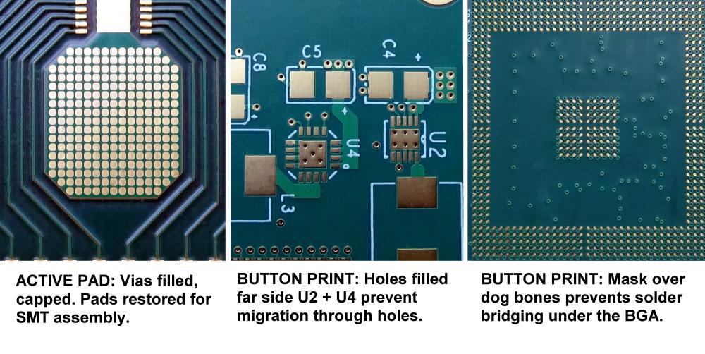
8. Hole Filling and Capping
Optional hole filling or capping material can be applied on vias as needed.
This sequence results in plated holes with copper barrel walls coated in soldermask becoming electrically conductive vias.
Key Via Design Parameters
Some key factors to consider when designing vias:
- Via Diameter – Determines current carrying capacity. Typical sizes are 0.3mm to 0.6mm.
- Hole Wall Thickness – Plating thickness should be ≥ 25um for reliability.
- Annular Ring Width – Ring of copper around via on each layer. IPC-2221 recommends ≥ 0.15mm annular width.
- Anti-pad Diameter – Copper area removed around via in signal layers to isolate via.
- Land Pad Diameter – Exposed via pad where hole breaks out on outer layers.
- Via Pitch – Spacing between adjacent vias in an array.
- Stacked Vias – Number of vias stacked vertically at one location.
- Barrel Fill Material – Air, resin or conductive material used to fill drilled hole.
Via Current Carrying Capacity
Vias can carry substantial current between layers owing to their plated copper barrel. The via current capacity depends on:
- Via barrel copper thickness – Thicker plating carries higher current
- Via diameter – Larger diameter hole has lower resistance
- Anti-pad size – Larger anti-pad provides more heat dissipation
- PCB copper weight – Heavier copper layers handle more current
- Hole plugging material – Conductive filled vias carry more current
Typical via current ratings are approximately:
- 0.15 mm via diameter – 0.5 A
- 0.2 mm via diameter – 0.7 A
- 0.3 mm via diameter – 1 A
- 0.4 mm via diameter – 1.5 A
This depends on PCB construction. Vias can safely carry higher currents with optimized PCB design.
Advantages of Smaller Diameter Vias
The continuing trend is to utilize smaller vias where possible. Some benefits of using smaller vias include:
- Higher Via Density – More vias can be placed in the same board area.
- Routing Channels – Provides space for routing signal traces between vias.
- Lower Capacitance – Decreases parasitic capacitance to ground plane.
- Lower Inductance – Reduces series inductance for bypassing applications.
- Lower Cost – Requires less plating metal resulting in cost saving.
- Fine Pitch Compatibility – Matches small pad pitches of fine-pitched components.
- High Speed Suitability – Minimizes stub effects of vias in high speed signals.
- Improved Impedance Control – Allows closer impedance matching for controlled impedance routes.
- Narrower PCBs – Permits thinner board widths by eliminating need for wide via spans.
Functions of Different Via Types

The main types of vias are utilized for the following typical functions in PCBs:
Through Vias:
- Interconnect signal layers
- Connect component pads to inner layers
- Distribute power from internal plane layers
Blind Vias:
- Fanout bottom side mounted devices to inner layer
- Route specific signals between required layers only
- Transition signals between fine pitch devices to maintain line width
Buried Vias:
- Interconnect internal power and ground planes
- Thermal vias to dissipate heat from inner layer power devices
- Reduce layer transitions improving signal quality
Role of Anti-pads
Anti-pads are the clearance areas where copper is removed around the via barrel on a signal layer:
- Provide isolation from copper planes adjacent to the via
- Prevent shorting between signal trace and via barrel
- Control impedance based on anti-pad size relative to trace width
- Reduce capacitive loading on signal traces from planes
- Help tuning via stub effects on high speed signals
- Improve manufacturability by giving tolerance around barrel
Typical anti-pad to via diameter ratios range from 1.0 to 1.5.
Stacked and Filled Vias
Stacked Vias consist of multiple vias vertically stacked at the same location through several PCB layers. Advantages of using stacked vias include:
- Carry higher current loads
- Provide low inductance robust connections
- Improve heat transfer between layers
- Achieve higher interlayer connection densities
- Enable large plane area isolation with stacked through vias
Filled Vias have their drill hole filled with conductive or non-conductive material after plating. Benefits of filled vias:
- Prevent debris, moisture and contaminant ingress
- Allows probing or placing components in vias
- Improves structural and mechanical integrity
- Provides electrical isolation with non-conductive fill
- Increases current capacity with conductive fill like copper paste
- Reduces moisture absorption and via fracture failures
Via Placement Principles
Guidelines for optimal via placement include:
- Minimize total via count and utilize stacking for robust connections.
- Place vias at component pins directly instead of relying on spoke routing whenever feasible.
- Route traces orthogonally when transitioning between layers using vias for shortest path.
- Avoid putting vias in high current power distribution paths. Use plane layers instead.
- Place thermal relief spokes at plane edges when connecting plane layers to avoid fractures.
- Keep high speed signal vias close to IC pins and avoid long stubs.
- Surround QFN/DFN component pads with ground vias for shielding EMI.
- Maximize distance between via fences used for plane isolation to minimize performance impact.
- Use symmetrical patterns on opposite sides when arraying vias for plane connections to avoid warping.
Selecting Via Technology
With higher performance requirements and densities, PCBs increasingly utilize advanced via fabrication technologies:
- Laser Drilled Vias – For <0.15mm vias where mechanical drilling is limited
- Microvias – Necessary for complex HDI designs (>20 layers)
- Buried Vias – Bluetooth and other RF designs requiring vias between inner layers
- Back-drilled Vias – Remove unused portion of long vias for RF and high speed boards
- Extended Fat Vias – Low inductance structures for power delivery
- Skip Vias – Improve routing flexibility on dense boards by skipping valid hole locations
Typical Via Defects and Failure Modes
Some common defects and reliability issues related to vias include:
- Open Vias – Lack of plating continuity causing open electrical connection.
- Underplated Hole Walls – Insufficient plating thickness leading to reduced conduction and reliability risk.
- Overplated Barrel – Excessive plating bulge obstructing trace routing.
- Burrs – Rough edges around drilled hole causing shorts.
- Skewed Holes – Drill misalignment relative to pad center causing reliability concerns.
- Cracks – Heat and moisture can cause fracture cracks in plated via structures impairing conductivity.
- Separation – Thermal cycling stress can cause separation between barrel and pad interfaces leading to electrical failure.
- Corrosion – Plated copper corrodes over operating lifetime due to moisture ingress degrading conductivity.
PCB Design Guidelines for Using Vias
Some key guidelines regarding via design and layout:
- Define different via styles with appropriate padstacks for through vias, blind vias and buried vias.
- Set minimum annular rings, hole size and anti-pad clearance rules based on board fabrication capabilities.
- Plan out preliminary via distribution and quantity during placement stage as this impacts routing.
- Route critical signals preferentially on inner layers first to minimize length and layer transitions through vias.
- Stack and fill vias where higher current capacity connections are needed.
- Increase anti-pad size on small vias used in RF and high speed circuits to control characteristic impedance.
- Do not share vias between analog and digital sections to prevent coupling of noise.
Conclusion
The via is a simple yet extremely versatile structure that makes multilayer PCB designs feasible. They enable vertical interconnections between layers for signals, power distribution and heat transfer. Appropriate application of different via types along with careful parameter selection is key to harnessing the advantages of vias while mitigating the impact of parasitics. With increasing performance requirements and shrinking geometries, PCB designers must master via design principles to create optimal designs balancing functionality, reliability and manufacturability.
Frequently Asked Questions on PCB Vias
Q1. What are the main advantages of using smaller diameter vias in a PCB?
Smaller vias allow higher via density, reduced capacitance, lower inductance, thinner boards, finer pitches and improved signal integrity which are all crucial for high speed designs.
Q2. When should filled vias be used instead of unfilled plated through holes?
Filled vias prevent debris ingress, allow probing, increase structural rigidity, provide isolation with dielectric fill, boost current with conductive fill, and reduce PCB moisture absorption.
Q3. How does the anti-pad diameter size around a via impact the PCB design?
Larger anti-pads provide better isolation from planes, reduced capacitance, improved impedance control and manufacturability, but also consume more board space.
Q4. What are some common defects and reliability issues associated with PCB vias?
Open vias, cracked barrels, poor plating, skewed holes, separation from pads, bulging barrel, hole corrision and fractures are some via related defects affecting reliability.
Q5. What are the main considerations when designing vias in a multilayer PCB?
Electrical connectivity, stackup spans, thermal heat transfer, carrying current levels, isolating planes, minimizing parasitics, controlling impedance and maintaining manufacturability should be considered.


