Printed circuit boards (PCBs) provide the interconnect foundation for electronics. A key role of the PCB is safely routing power throughout the system. For high power applications, factors like trace width must be carefully designed to handle required currents.
Trace width has a major impact on current capacity. Wider traces allow more current without excessive heating. But what is the relationship between trace width and current for common PCB conductor thicknesses?
This article explores PCB trace width versus current, with a focus on high power capacity design. It provides:
- Overview of key factors influencing trace current
- Trace width vs. current tables
- Guidance for designing high power traces
- Methods for handling very high currents
- Example layout scenarios
- Frequently asked questions
By understanding how trace width influences current capacity, designers can create robust, safe PCB power networks for high power electronics.
Factors Influencing Trace Current Capacity
Several variables affect the maximum current a PCB trace can handle:
Conductor Thickness
Thicker copper carries current more efficiently due to lower resistivity. Common thicknesses are 1oz (35μm), 2oz (70μm) and 3oz (105μm).
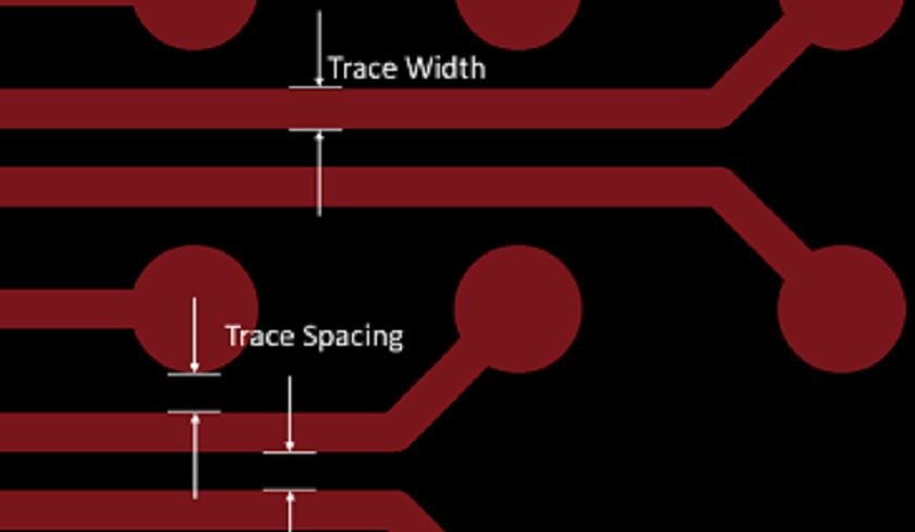
Conductor Width
Wider traces have a reduced current density and lower resistance allowing greater current flow.
Conductor Length
Longer traces increase resistance and heating proportional to length. Short, wide traces handle more current.
Copper Type
Copper purity and rolling direction impact resistivity. Rolled annealed copper offers the best conductivity.
Trace Temperature Rise
The acceptable temperature rise limits current. Temperature directly influences copper resistivity.
PCB Dielectric Material
The PCB laminate affects heat transfer away from the trace to limit temperature rise.
With an understanding of these factors, appropriate trace widths can be calculated to carry required board currents.
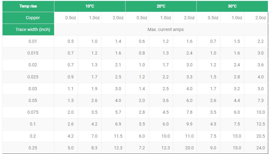
Trace Width vs. Current Tables
Trace width determines current capacity for a given conductor thickness. The table below provides typical maximum current values for common PCB trace widths and copper weights:
| Trace Width | 1 oz Copper | 2 oz Copper | 3 oz Copper |
|---|---|---|---|
| 10 mils | 1.2 A | 2 A | 3 A |
| 15 mils | 1.7 A | 3 A | 4 A |
| 20 mils | 2.2 A | 4 A | 5 A |
| 25 mils | 2.8 A | 5 A | 6 A |
| 30 mils | 3.3 A | 6 A | 7 A |
| 40 mils | 4.4 A | 8 A | 10 A |
| 50 mils | 5.5 A | 10 A | 13 A |
| 75 mils | 8.2 A | 15 A | 18 A |
| 100 mils | 11 A | 20 A | 25 A |
| 150 mils | 16.5 A | 30 A | 37 A |
| 200 mils | 22 A | 40 A | 50 A |
These values assume an ambient temperature of 25°C with no additional heat sinking or airflow. Length is restricted to 3 inches.
As shown, increasing trace width rapidly allows higher current capacity for a given copper weight. Additional cooling extends capacity further.
Design Guidance for High Current Traces
To leverage wider traces for high current PCBs, keep several guidelines in mind:
- Use thicker 2oz or 3oz copper layers for high current routes
- Maintain short trace lengths to minimize resistance
- Locate power traces inner layers for heat spreading into ground planes
- Parallel multiple traces if a single wide trace is inadequate
- Utilize existing copper shapes for power instead of removing copper
- Provide sufficient clearance around traces for heat dissipation
- Incorporate thermal reliefs and spoke patterns when needed
- Add component heat sinks to supplement trace cooling
Careful planning following these principles allows effective utilization of available space for wide traces that deliver substantial current.
Handling Extreme Currents
When high current requirements exceed standard PCB trace capabilities, several approaches are available:
Metal Core Boards
Insulated metal core PCBs use thick metal layers for high power routing. This effectively heatsinks traces while containing electromagnetic interference.
Bus Bars
Thick metal bus bars integrated directly into PCB provide very low resistance connectivity for hundreds of Amps.
Litz Wire
Litz wires employ many fine gauge insulated strands to distribute current and cancel inductance for high frequency power delivery up to hundreds of Amps.
Solid Metal Layers
Entire metal layers on special PCBs can be used for very high current power distribution over 10,000 A/cm2.
Hybrid Circuits
Combining standard PCBs with external cabling, flex circuits, or direct metal connections provides additional current capacity.
Active Cooling
Fans, liquid cooling, and heat sinks remove heat allowing higher trace current for a given size.
So a range of solutions can push trace current well beyond standard limits to meet the most demanding power design needs.
Example Trace Width Scenarios
To make these concepts more concrete, here are example PCB current carrying scenarios and resulting trace width needs:
Scenario 1
- Supplying 12V at 10A to a motor driver module
- Using 2oz copper for inner layer power distribution
- Total trace length around 2 inches
Solution:
From table, 2oz trace needs to be 150mils wide minimum to carry 10A for this short length.
Scenario 2
- Routing 5V standby power to ICs at 2A total load
- Using 1oz copper on surface layers
- Traces around 4 inches long
Solution:
2A over 4″ requires around 60mil trace width on 1oz copper per table.
Scenario 3
- Distributing high current 5V to multiple processors at 150A total
- Using thick 3oz copper with air cooling
- Length about 1 inch
Solution:
150A exceeds normal PCB traces. A bus bar or metal substrate is a better solution. If on PCB, parallel traces or Litz wire requires.
This illustrates how to appropriately size traces for target current loads based on table data.
Frequently Asked Questions
Some common questions that arise when designing trace width for high currents:
How are the allowable current values in the table calculated?
The values derive from IPC-2152 standard trace/space design calculations based on heat rise and ampacity.
Do I have to stay under the table values?
It is recommended to stay within the guidelines to ensure safe heat dissipation. Exceeding the values risks overheating damage.
Can traces handle occasional current spikes above the table values?
Occasional minor transients are generally okay but sustained excessive current will overheat traces.
What is the impact of room temperature on the table?
Higher ambient temperatures reduce allowable trace current. De-rating factors may need to be applied if room temperature exceeds 25°C.
When is it better to use an external wire instead of a wide trace?
For very high current loads, thick external cabling may be preferable to wide PCB copper pours due to flexibility and cooling benefits.
In summary, the table values provide a useful guideline but further analysis may be required for specialized high power applications.
Conclusion
Trace width has a large impact on allowable printed circuit board current. For high power PCBs, maximizing trace width is key within the constraints of the layout. Wider traces proportionally increase capacity but must be carefully optimized against other routing considerations.
This guide provides a useful reference for estimating required trace widths based on expected currents. However, additional thermal modeling and design margin is recommended when pushing limits. By planning for wide, short traces in advance, even extreme power levels can be accommodated on a PCB through careful design.


