Vias play a critical role in printed circuit boards (PCB) by facilitating interconnections between layers to route signals and distribute power. The current carrying capacity of vias must be adequately designed to ensure power integrity and prevent reliability issues due to overheating.
This article provides a comprehensive guide on how to analyze, estimate and design the maximum current that can be safely handled by vias based on parameters such as via construction, PCB design, application environment and reliability requirements.
Best practices to optimize and increase via current capacity are also detailed.
Importance of Via Current Carrying Capacity
The main considerations regarding via current capacity include:
- Preventing Overheating Damage: Vias exceeding their current rating can overheat causing permanent damage to PCB.
- Avoiding Board Failures: High current vias flowing too much current leads to reduced reliability and potential field failures.
- Power Distribution: Vias must be designed to carry expected current loads between power and ground layers.
- Signal Integrity: Inadequate current capacity causes voltage drops affecting signal performance.
- Safety: Overheating poses risks of fires or burns. Vias current capacity impacts safety.
- Performance: Optimized vias carrying maximum possible current enhances circuit performance.
- Cost: Redesigning boards due to insufficient via current capacity increases PCB cost.
Factors Impacting Via Current Capacity

The maximum current a via can handle depends on several PCB design, material and environmental factors:
Via Dimensions:
- Via barrel diameter
- Hole wall plating thickness
- Anti-pad size
PCB Stackup:
- Copper layer thickness
- Amount of copper heat sinking area
- Location in layer stackup
Operating Environment:
- Ambient temperature
- Altitude affecting air density for cooling
Reliability:
- Desired product lifetime
- Allowable via temperature rise
Application Type:
- AC vs DC current
- Transient vs continuous current
Calculating Via Current Carrying Capacity
The via current capacity can be calculated using the following thermal resistance model:
Imax = (ΔTmax / RθJA)1/2
Where:
Imax = Maximum allowable current through via (Amps)
ΔTmax = Maximum permitted via temperature rise (°C)
RθJA = Thermal resistance from via barrel to ambient (°C/Watt)
The key steps are:
- Determine maximum allowable via temperature rise based on:
- Via plating material properties
- PCB laminate glass transition temperature
- Reliability failure rate models
- Calculate via barrel to ambient thermal resistance RθJA
- Compute maximum current using Imax formula
This provides the theoretical current capacity. Appropriate design margin and derating should be applied for real-world conditions.
Calculating Via Thermal Resistance

The via thermal resistance RθJA depends on various thermal resistances:
RθJA = RθJC + RθCS + RθSA
Where:
RθJC = Via barrel junction to pad Cu resistance
RθCS = Cu pad spreading resistance
RθSA = PCB surface to ambient air resistance
Each component can be estimated as:
Via Barrel Resistance RθJC:
RθJC = ln (Dout/Din) / (Π * Kcu * L)
Dout = Outer diameter of via barrel
Din = Inner diameter of via hole
Kcu = Thermal conductivity of Cu
L = Length of via barrel
Copper Spreading Resistance RθCS:
RθCS = 1 / (Π * Kcu * sqrt(A))
A = Area of Cu heat spreading
PCB Surface Resistance RθSA:
RθSA = 1 / (hconv * A)
hconv = Convection coefficient
A = PCB surface area
This provides the total thermal resistance from the via barrel through the PCB layer to the ambient air.
Sample Via Current Capacity Calculation

Here is an example via current capacity calculation for a typical 0.3 mm diameter through hole via:
Given:
Via diameter = 0.3 mm
Via plating thickness = 25 μm
Ambient temperature = 55°C
Max. via temperature rise = 15°C
PCB Cu thickness = 1 oz (35 μm)
PCB area for heat spreading = 20 mm x 20 mm = 400 mm2
Thermal Resistance Calculation:
RθJC = ln (0.36/0.3) / (3.14 * 385 * 0.0025) = 48 °C/W
RθCS = 1 / (3.14 * 385 * sqrt(400)) = 0.06 °C/W
RθSA = 1 / (10 * 400) = 0.025 °C/W
Total RθJA = 48 + 0.06 + 0.025 = 48.085°C/W
Current Capacity:
Imax = (15 / 48.085)^0.5 = 0.7 A
Therefore, max current capacity is 0.7 A for this via construction.
Via Current Capacity Table
The current rating of plated through hole vias for a typical PCB construction is provided below as a reference guideline:
| Via Diameter | Max Current |
|---|---|
| 0.15 mm | 0.5 A |
| 0.2 mm | 0.7 A |
| 0.3 mm | 1 A |
| 0.4 mm | 1.5 A |
| 0.5 mm | 2 A |
| 0.6 mm | 2.5 A |
| 0.8 mm | 4 A |
| 1.0 mm | 6 A |
Increasing Via Current Capacity
Here are some techniques to enhance via current capacity in a PCB design:
Increase Via Barrel Diameter
- Use larger hole diameter to reduce resistance
- Balances capacitance and inductance effects
Increase Via Barrel Thickness
- Specifies thicker copper plating on hole wall
- Reduces conduction losses through barrel
Enlarge Anti-Pad Diameter
- Provides more copper annulus for heat spreading
- Prevents barrel overheating damage
Add More Vias in Parallel
- Distributes current across multiple vias
- Increases total cross sectional area
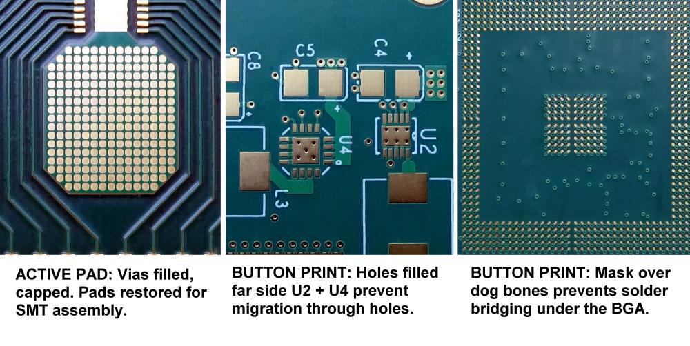
Use Filled and Capped Vias
- Filled vias provide more heat spreading
- Capped vias prevent solder wicking into hole
Utilize Thicker Copper PCB Layers
- Heavier copper foils conduct heat better
- Reduce spreading resistance into plane layers
Increase Thermal Plane Area
- Maximize copper heat sink area with thermal relief voids
- Improves lateral heat spreading from vias
Optimize PCB Layer Stackup
- Place high current vias closer to surface layers
- Add extra layers to reduce spreading resistance
Changing Via Current per Layer in Multilayer PCBs
Vias interconnect different combinations of layers in multilayer boards. Some guidelines for handling via currents based on layer span are:
Surface Layer Vias
- Highest current capacity vias with maximum heat spreading
- Good for decoupling capacitors carrying high AC currents
Mid-layer Vias
- Moderate current capacity due to smaller copper heat sinks
- Suffer from trapped heat without air circulation
Deep Inner Layer Vias
- Lowest current capacity due to thermal resistance through stackup
- Should only be used for low current connections
Partial-depth Vias
- Current capacity depends on the layer depth they connect
- Blind and buried vias below surface have lower current rating
By matching required currents to via spans through the layer stackup, the current carrying capability can be optimized.
Managing AC Currents in Vias
Vias carrying alternating currents require additional design considerations:
Skin Effect
- AC currents concentrate near barrel surface
- Reduces effective cross sectional area
- Wider shorter vias mitigate skin effect
Proximity Effect
- AC currents distribute non uniformly
- Shifts current density lowering capacity
- Place AC current vias away from other vias
Inductive Reactance
- Changes current phase through via
- Causes localized hotspots around barrel
- Requires larger anti-pads to handle hotspots
Resonance Issues
- AC currents can excite resonant modes
- Leads to ringing creating EMI concerns
- Affects high frequency or very fast rise time currents
Proper modeling and simulation of these effects is necessary to design reliable high frequency AC current vias.
Managing DC Currents in Vias

DC currents also require certain design considerations for vias:
Electromigration
- DC current causes copper ion drift over time
- Can lead to conductor failure or voids
- Limit DC current density to ≤ 500 mA/mm2 of cross section
Thermal Cycling
- Repeated heating and cooling cycles
- Induces thermal expansion stresses
- Fatigue cracking or pad lift off issues
- Filled vias and larger annular rings help
Galvanic Corrosion
- Disparate metals in via galvanic pair
- Causes accelerated corrosion damage
- Apply compatible platings like Au over NiPd in barrel
Via Current Density
- Ensure even DC current distribution among vias
- Avoid hotspots from imbalanced flow
- Model both DC and AC current effects
External Magnetic Fields
- Circulating currents induced by DC current
- Concentrates currents on one side
- Orient orthogonal to magnetic field vectors
High Current Via Design Examples
Here are some examples of implementing high current capacity via design techniques:
Power Supply input filter
- 5mm diameter filled solid vias to handle 50A input
- 10 vias x 5 mm diameter = 15 mm2 total area
- Filled with conductive epoxy to increase cross section
LED Matrix Panel
- 1.5mm diameter plated through hole vias
- 75 vias distributed uniformly
- Handles total 25A current across array
- Vias spaced with ground returns to control impedance
High Power Motor Driver
- Surface layer current sense resistors
- 0.5mm blind vias to inner ground plane
- Blind vias avoid full stackup thermal resistance
- Non conductive filler prevents solder wicking
Automotive PCB
- 0.3mm vias connecting -40°C cold side to +105°C hot side
- Filled vias prevent solder leaching issues
- Large annular rings reduce crack failures under thermal cycling
Design Verification for Via Currents

To ensure the designed vias can safely handle the intended currents, rigorous verification through simulation, analysis and testing should be performed:
- Worst Case Transient Analysis: Verify peak transient current spikes do not exceed ratings.
- Electro-Thermal Simulation: Compute detailed thermal profile and heating effects under current loads.
- Power Integrity Analysis: Confirm acceptable voltage drop across vias carrying DC currents.
- Signal Integrity Modeling: Analyze impact of AC currents on impedance, EMI and coupling.
- Sensitivity Analysis: Model performance sensitivity to variations in design parameters.
- Design Margin Allocation: Apply margins to account for derating, tolerances and uncertainties.
- Prototyping Measurements: Empirically measure temperatures and voltage drops under load conditions.
- Accelerated Lifetime Testing: Assess robustness under extreme temperature cycling, voltage, humidity etc.
A comprehensive verification methodology ensures the designed vias provide reliable operation over the product lifetime under varying conditions.
Conclusion
Vias play a critical role in routing signals and distributing power across layers in complex PCB designs. However, exceeding the current carrying capacity of vias can compromise reliability. A robust design process encompassing electrical, thermal and mechanical analysis along with verification testing is essential to determine the maximum safe current for vias. Techniques like increasing barrel thickness, thermal heat sinking and using filled vias further help optimize the current handling capability. Checking adequacy of vias early in the design flow using modeling, simulation and prototyping prevents expensive failures arising from undersized vias in manufactured boards.
Frequently Asked Questions on PCB Via Current Capacity
Q1. Why is it important to design adequate via current capacity in PCBs?
Vias carrying excessive current overheat causing damage or reduced reliability. Properly sizing vias prevents failures from insufficient current capacity.
Q2. What PCB design factors influence the maximum current carrying capacity of vias?
Via diameter and plating thickness, anti-pad size, Cu layer weights, heat sinking area and ambient temperature primarily impact the current capacity.
Q3. How does AC current handling capability of a via differ from DC current capacity?
Skin effect, proximity effect and resonance concerns need additional design considerations for AC currents compared to DC capacity.
Q4. Do vias spanning different combinations of layers in a multilayer PCB have different current ratings?
Yes, vias between surface layers handle highest currents whereas deep inner layer vias have the lowest current capacity.
Q5. What kinds of analyses and verifications are used to validate via current capacity?
Simulations, thermal modeling, power integrity checks, signal integrity analysis, sensitivity studies, prototyping measurements and accelerated testing should be used.


