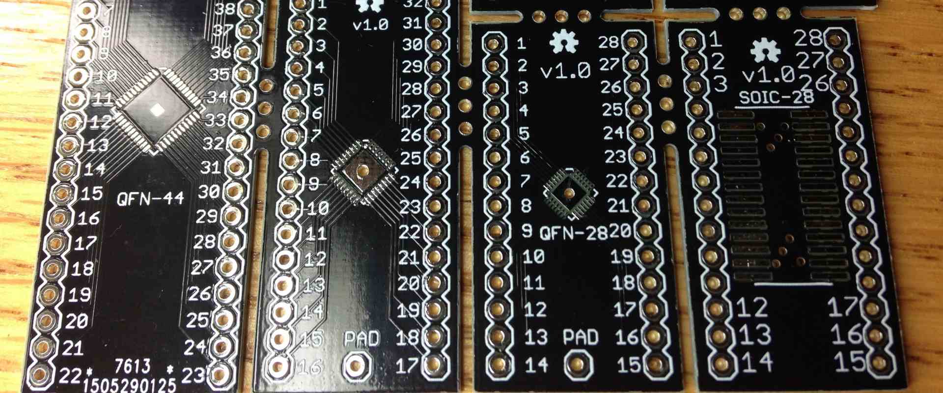
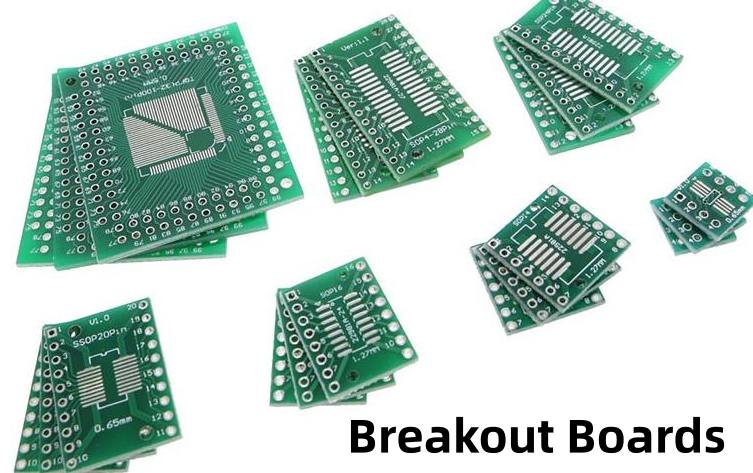
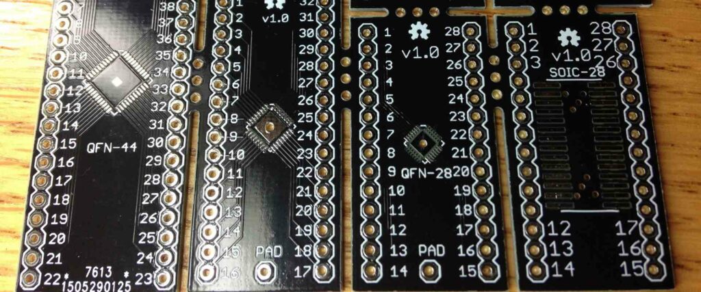
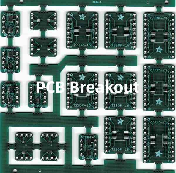
A SMT breakout board refers to a small printed circuit board designed to convert the fine pitch of surface mount component terminals into wider through-hole pins or solder pads to facilitate prototyping, testing, and debugging.
Breakout boards simplify integration with devices having dense ball grid arrays (BGAs), land grid arrays (LGAs), quad flat packages (QFPs), or other challenging surface mount footprints unsuited for breadboarding techniques. They are an indispensable tool enabling accessible interface with advanced components for lower cost and faster time to market.
Key Attributes of Breakout Boards
Effective SMT breakout boards have several notable characteristics:
- Designed for a specific target surface mount component package
- Reroute component terminals to 0.1” or larger pitch access points
- Offer standalone PCB handling independent of target device
- Allow pressure mounting or soldering of target component
- Support multiple orientations and cable connections
- Provide test points and debugging features
Common materials include FR4 glass epoxy and flexible PCB substrates to balance ruggedness, electrical performance, and cost factors.
Why SMT Breakout Boards Are Necessary
Several factors necessitate using breakout boards to leverage modern components:
Ultra Fine Pitch ICs
Printed circuits with densities exceeding 500 I/O pins in a grid array area smaller than 1 square inch require substrate rerouting to a workable pitch.
Miniaturization Trends
Components like wafer scale sensors continue shrinking far below the realm of practical direct prototyping ability despite complex internal capabilities.
High Frequency Optimized Packages
Emerging packaging achieves 40+ GHz operation yet has interconnects measured in microns prohibiting direct access with lab equipment.
Commercial IP Protection
Many commercial components utilize package obscuration techniques protecting their full feature set pending appropriate security key activation. Breakout access defeats this.
Types of Breakout Boards
Many SMT breakout board variants exist targeting different applications:
Basic Debugging Boards
These most common boards simply match the target device footprint and break signals out to 0.1” headers. Key for initial prototype validation and simple debugging access with an oscilloscope or multimeter probes.
Expanded Capability Boards
Additional PCB area allows integrating supplementary circuitry including voltage regulation, oscillators, decoupling, and reference clocks tailored for the target subsystem. Supports complex peripheral integration minimizing external bills of materials.
Active Probing Boards
Dedicated high frequency solder down probes route signals to precision RF measurement equipment while specialized launch structures maintain signal integrity up to microwave bands. Permit previously impossible insight into internal IC waveforms.
Programmable Logic Boards
Integration of CPLD or FPGA devices on breakout boards facilitates powerful real time decoding of interface buses, performing stimulus response validation, and manipulating internal status/control registers through instantiated testbench IP.
Interposer Boards
Cutting edge breakouts utilize interposer technology embedding ultra-fine multi-layer routing inside the PCB substrate enabling escape of the most aggressive packages on market.
Typical Breakout Board Usage Models
Breakout boards see frequent usage across several standard workflows:
Laboratory Prototyping
Bench characterization and validation of components lets engineers explore full operation ranges before integration into enclosed production systems.
Design Verification
Test engineers leverage breakouts to access internal defaults allowing corner case product testing impossible otherwise due to self diagnostic disables. Significant cost and schedule advantages result.
Failure Analysis
When issues emerge in systems, breakout boards permit probing with lab equipment to localize fault sources facilitating rapid root cause diagnosis and repair recommendations.
Secure Applications
Breakout access defeats commercial package protections permitting usage of devices exceeding their intended capabilities in government or scientific projects where cost is no object.
Small Batch Testing
Engineers qualify small production batches by performing parametric measurement and burn-in qualification over wide ambient and power delivery scenarios difficult within enclosed products.
Technical Considerations for Breakout Implementation
Several key technical factors guide the design process when architecting breakout boards:
1. Matching Component Footprint
Accurately capturing pad geometries, solder mask profiles, and density enables reliable mounting of the target package.
2. Letterbug Orientation
Maintaining letterbug positioning from the native PCB allows quick signal mapping through consistent pinouts. Rotating letterbugs requires constant pin mentally translation.
3. Decoupling Integration
Strategic onboard power filtering and decoupling mimics target application environments ensuring stable electrical operation.
4. Impedance Control
Controlling trace geometries, vias, and ground planes sets matched impedances facilitating reliable interfacing at microwave interface speeds.
5. Vertical Interconnection
Vertical board stacking and high density connectors maintain breakout usability even as hidden PCB real estate shrinks available area.
Comparison of Breakout Boards vs. Related Solutions
| Parameter | Breakout Boards | Interposer Boards | Test Socket Boards |
|---|---|---|---|
| Adaptability | Fixed | Device Specific | Generic |
| Target Device Connection | Soldered | Soldered | Zero Insertion Force Pins |
| Frequency Support | ~5 GHz | 10 – 100 GHz | 500MHz – 1GHz |
| Routing Flexibility | Medium | Ultra High Density | Limited, Edge Only |
| Device Powering | Full, Onboard Regulation | Little/No Onboard Power | External Requirement |
| Cost | Low-Medium | Very High | Medium-High |
Conclusion
In summary, SMT breakout boards deliver indispensable capabilities allowing engineers to unlock the full potential of contemporary electronic components through enabling prototyping, test, and debugging access. As production devices continue getting smaller while integrating skyrocketing gate counts, leveraging clever rerouting and interconnection techniques guarantees innovative organizations remain on the cutting edge rather than relegated as passive early adopters. Preeminent access makes breakout boards the last line of defense ensuring project vision stays on schedule meeting stakeholder demands even as Moore’s Law progresses.
Frequently Asked Questions
How are breakout boards fabricated for volume production components not released yet?
Footprint and terminal information is obtained by engineers through package drawings, scanning quad flat packages with high powered microscopes to determine pinouts, and licensing component simulation packages from the vendor to capture exact PCB layout data.
What techniques allow interfacing test equipment as packages shrink below 100 microns scale?
Precision probes coupled to substrate interposers or sophisticated launch structures maintain matched impedance to active equipment inputs while positioning probe tips precisely across tiny package bumps. Custom probe cards leverage these compounded techniques maximizing visibility.
How do breakout boards prevent damaging sensitive components under test?
Protection devices including transient blocking diodes, transient voltage suppressor diodes, and surge stopping fuses get integrated into breakouts safeguarding against inadvertent power abnormalities reaching components allowing investigation right to normal operational limits.
Why don’t semiconductor vendors support open breakout board ecosystems themselves?
Competitive realities mean leveraging package obscuration, wafer scribing, focused ion beams, and other techniques deliberately handicapping maximum performance ships commercially unless security techniques activate. Vendors correctly view motivated breakout designers circumventing protections counterproductive to profit strategies by empowering discounted segments.
What breakthroughs further enhance SMT breakout board capabilities on the horizon?
3D printing high density multi-scale interconnect substrates enables ad hoc bridging to emerging wafer scale components. Innovations embedding active logic reconfigurably helps custom tailor breakouts optimally paralleling any target architecture for fast component investigation minus silicon respins.


