Introduction
A PCB footprint defines the pattern of copper pads, traces, and other features that represent a component on the board layout. Footprints precisely specify the land pattern geometries and dimensions required to successfully solder components and route connections to them. Incorrect footprints are a common source of issues during PCB assembly and manufacturing.
This article provides clear guidelines on designing footprints that accurately match component leads and enable defect-free, reliable solder joints. We will examine recommended dimensions, rules-of-thumb, and design practices for through-hole, surface mount, and unconventional component footprints. Learning proper footprint design principles will improve manufacturing outcomes and avoid costly mistakes at the PCB fabrication stage.
Through-Hole Component Footprints
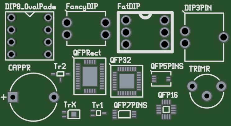
Let’s first review recommended practices for through-hole component footprints:
Pad Dimensions
- Pad diameter should match hole size plus 2x the annular ring width
- Typical annular ring is 0.2-0.5mm beyond hole diameter
- Adjust pad size based on; hole size, lead thickness, solder volume needed
Pad Spacing
- Minimum spacing between pad edges is 1mm (40 mils)
- Increase spacing in high voltage or solder-bridging prone areas
Pad Shapes
- Standard pads are circular but can optionally be rounded rectangles
- Give rectangular pads rounded corners to avoid stress points
Thermal Relief Pads
- Optional spokes connect pad to plane to reduce heat conduction
- Used for thermally sensitive components like LEDs
Following minimum dimensions and clearances prevents tombstoning and bridges.
Surface Mount Footprints
For surface mount components:
Pad Dimensions
- Match pad length and width to component termination sizes
- Add 0.5 to 1mm clearance between pads
- Control pad height vs width ratio to optimize tombstoning resistance
Pad Patterns
- Two pad patterns are most common:
- Straight – pads on opposite sides
- Angled – pads offset on diagonals
Courtyard Area
- Add 0.5mm clearance around body for pick-and-place clearance
- Increase for large or high profile components
Thermal Pads
- Multiple vias help conduct heat from ground pad
- Optionally cover with paste mask opening for solder
Careful sizing and patterns avoid shorts while optimizing solder volume.
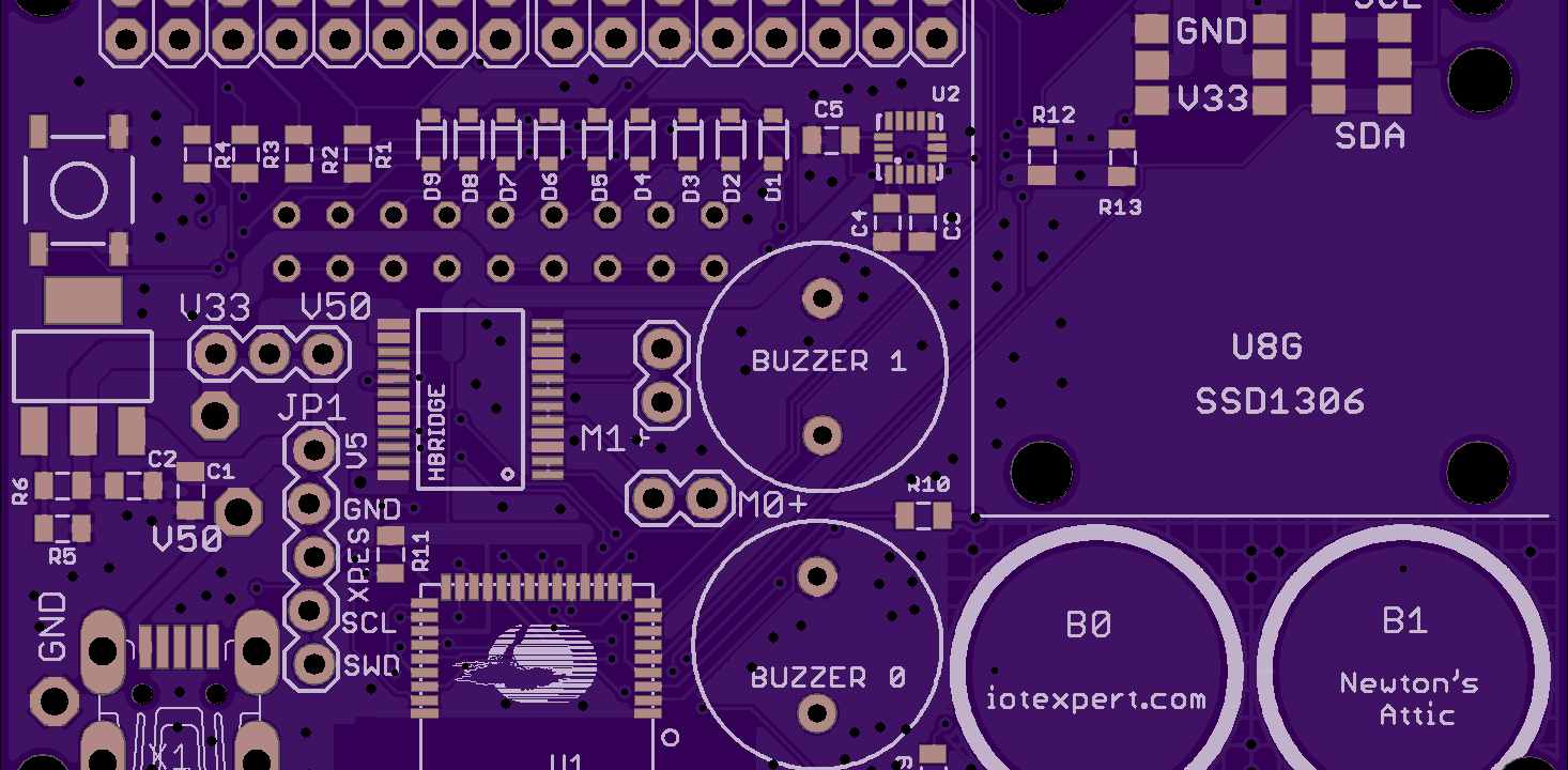
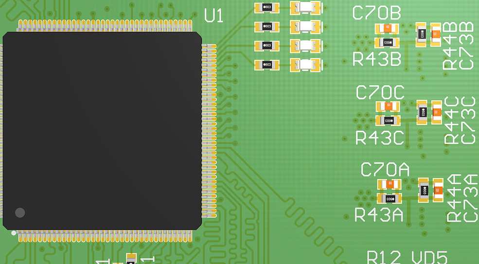
IC Packages Footprints
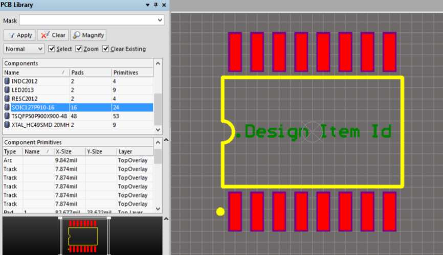
Integrated circuits in packages like QFP, SOP, and BGA require additional considerations:
Pad Dimensions
- Match sizes to manufacturer recommendations
- May require mingling of multiple pad sizes on single package
Pitch
- Follow standard pitch for package type
- QFP pads typically 0.5mm pitch
- BGA under 1.0mm
Thermal Pad
- Large ground pad underneath
- Multiple vias for heat dissipation
Pin 1 Indicator
- Chamfered rectangular pad indicates pin 1 location
- Assists visual inspection and orientation
Row Spacing
- Include standard lead row spacing for package
- Allow pick-and-place clearance between rows
Following industry conventions for common package styles avoids defective mounting and soldering.
Additional Pad Design Elements
Some additional pad features include:
Solder Mask Expansions
- Enlarge mask opening beyond pads to improve solder spreading
- Typical expansion is 0.2mm beyond pads
fiducials
- Small pads around perimeter provide component placement reference points
Assembly Notches
- Small cutouts that align with tooling pins during fabrication
Text Markings
- Reference designator, polarity markings, pin numbers etc.
These improve assembly alignment, accuracy, and inspection.
Footprint Simulation
Validating footprints with modeling and simulation helps avoid manufacturing issues:
3D Model Viewing
- Import step models to visually check clearances
Solder Bead Modeling
- Simulate reflow with realistic solder surface tension
DRC Rules
- Check minimum spacing, annular ring violations
Thermal Simulation
- Verify heat dissipation capacity for ground pins
While time-consuming, simulation provides added assurance of manufacturability before reaching the assembly house.
PCB Library Management
Well-constructed component libraries are essential for efficient design:
Parameterized Footprints
- Define generic footprints adjusted by variables
Manufacturer Validation
- Confirm footprints match datasheet recommendations
Single Source Library
- Consolidate verified footprints in a single source library
Revision Control
- Track footprint changes through PCB version control
A properly validated library avoids scrambling to fix incorrect footprints later in the development process.
Conclusion
In summary, designing correct PCB footprints requires attention to the precise mechanical details of component terminations and lead configurations. Following standards, simulating for manufacturability, and centrally managing validated footprints reduces damaging errors reaching assembled boards. While proper footprint design demands precision and care, mistakes caught late can lead to far greater costs in manufacturing re-spins and production delays. Investing effort upfront to learn and implement strong PCB library management will pay dividends across the entire electronics project development lifecycle.
Frequently Asked Questions
Q: What is the optimal pad shape for surface mount components?
A: Rectangular SMD pads with rounded corners are generally preferable. The rounded corners help prevent stress concentrations and fracturing.
Q: What clearance should separate exposed pad edges from housing?
A: A minimum clearance of 0.25mm between component body edges and exposed pads is recommended to prevent potential electrical shorts.
Q: How are thermal relief connections designed?
A: Thermal reliefs use thin traces or multiple small pads connected to a ground plane. This allows electrical connection while reducing conductive heat transfer.
Q: Can solder mask expansions replace thermal relief connections?
A: No, solder mask expansions only help solder wetting. Thermal reliefs are still needed for electrical ground connections that limit excess heat conduction.
Q: What is the benefit of fiducials on PCB footprints?
A: Fiducials provide clear visual reference points for alignment during fabrication and assembly. This improves precision of pick-and-place machines and routing equipment.


