Introduction
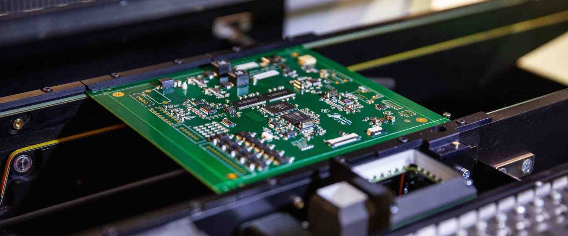
Printed circuit board assembly (PCBA) is the process of soldering or assembling electronic components to a PCB or printed circuit board. It involves mounting and soldering components like capacitors, resistors, integrated circuits (ICs), transistors, and other parts onto the PCB. The completed PCB assembly is a major component of electronic devices and equipment.
The PCBA process is an intricate and precise procedure that requires expertise, training, and the right tools and equipment. This step-by-step guide will walk you through the typical stages and key steps involved in assembling a PCB from start to finish.
Overview of the PCBA Process
The typical PCBA process comprises the following key stages:
- Solder Paste Printing
- Component Placement
- Reflow Soldering
- Inspection and Testing
- Repair and Re-work
- Conformal Coating
- Final Testing and Quality Inspection
This sequence of manufacturing stages allows efficient and high-quality population of components on PCBs. The sections below will examine each of these PCBA process stages in greater detail.
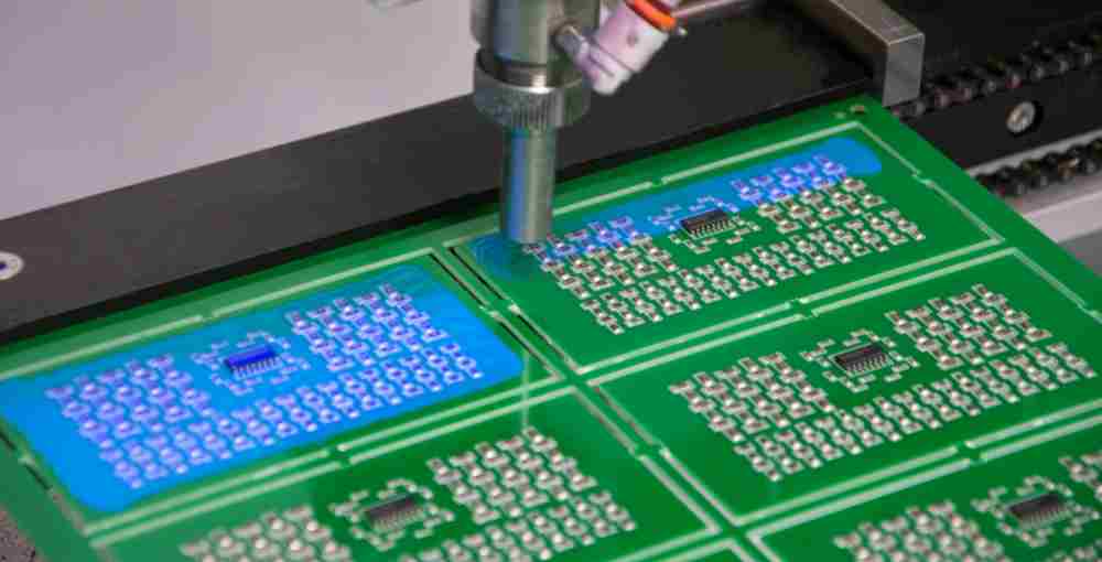
Stage 1: Solder Paste Printing
Solder paste printing is the first step of the PCBA process. It involves applying a controlled amount of solder paste on the PCB pads and lands.
Some key steps in solder paste printing are:
- PCB Preparation – The bare PCBs are cleaned, pre-baked, and prepared for solder paste printing.
- Stencil Alignment – The solder stencil is carefully aligned over the PCB to ensure accurate transfer of solder paste.
- Solder Paste Dispensing – Solder paste is dispensed onto the stencil surface usually by an automatic solder paste printer. The paste is usually an alloy of tin and lead.
- Solder Paste Transfer – The solder stencil is lowered and pressed onto the PCB surface to transfer the paste onto the pads.
- Stencil Cleaning – After the print stroke, the stencil is thoroughly cleaned to remove any residual paste.
- PCB Inspection – The PCB solder paste deposits are inspected under a microscope or AOI (Automated Optical Inspection) machine.
Proper solder paste printing ensures correct mounting and electrical connection of components during reflow soldering. Below is a table summarizing the key solder paste printing parameters:
| Parameter | Description |
|---|---|
| Solder Paste Type | Most common are Tin-Lead, Lead-Free solders. Metal alloy paste containing flux. |
| Aperture Design | Shape and size of stencil openings match pads. |
| Print Speed | 25-150 mm/sec, depending on printer. |
| Print Pressure | 1-2 kg of force per cm of squeegee length. |
| Paste Transfer Efficiency | >95% recommended. |
| Paste Height | Should be 150-250 μm after transfer. |
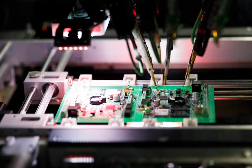
Stage 2: Component Placement
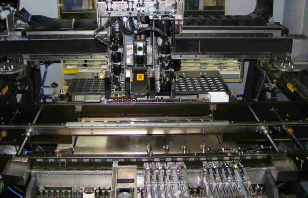
Component placement is the process of mounting the various electronic components onto the PCB sites with solder paste deposited. The steps include:
- Bill of Materials (BOM) – The types and quantities of components required for the PCB assembly are detailed in the BOM document.
- Component Preparation – The components are prepared based on specifications – leads straightened, formed, cut, etc.
- PCB Fixturing – The board is properly fixed in position on the conveyorized platform.
- Automatic/Manual Placement – Components are placed accurately on the right polarity pads either manually or using automatic pick-and-place machines.
- Adhesive Dipping – Some components like large connectors are secured on PCBs using adhesives by adhesive dipping before soldering.
The major factors considered during component placement are:
- Component outlines – shape, size, lead pitch
- Pad size, position – component-pad alignment
- Polarity – placing components in the right orientation
- Sequence of population – smallest to larger components
While manual placement uses human operators, automated pick-and-place systems are ideal for fast, high-volume PCB assembly. They can place 25,000-50,000 components per hour.
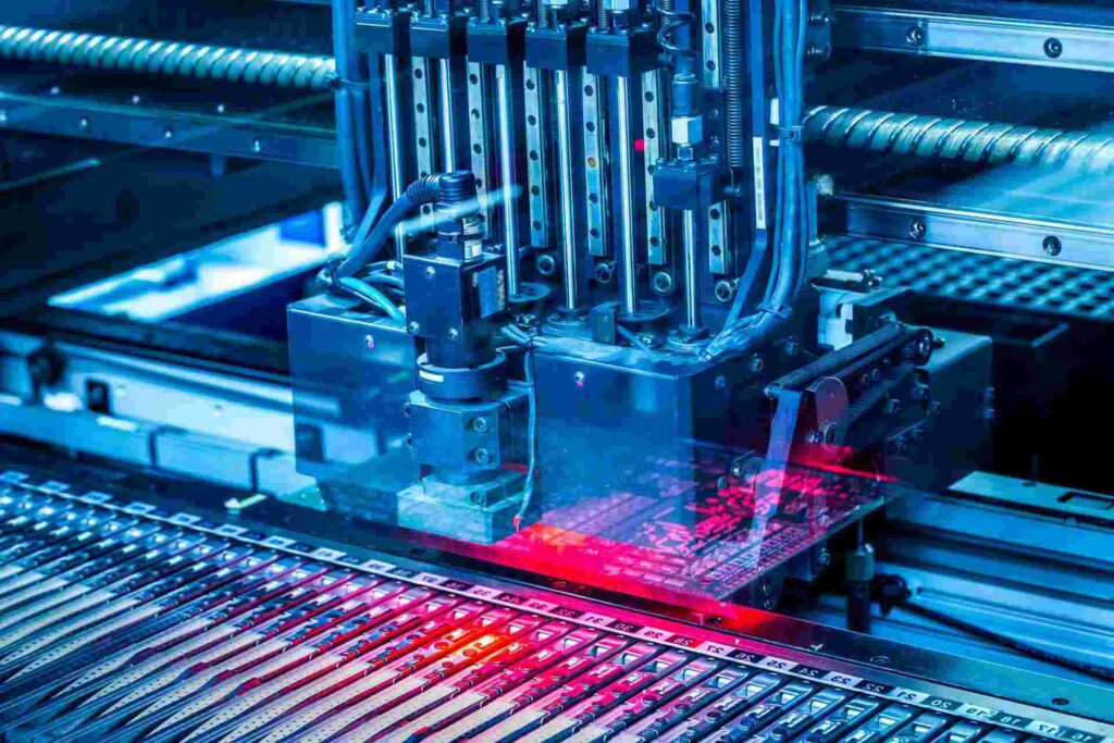
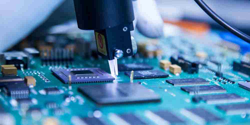
Stage 3: Reflow Soldering
Reflow soldering is the process of forming reliable electrical and mechanical joints between components and the PCB board by controlled heating and melting of solder. The stages in the reflow process are:
a. Preheating
The PCB assembly is slowly preheated to about 150°C to evaporate volatile flux constituents and prevent thermal shock to components.
b. Soaking
The temperature is held between 150-200°C for about 60-120 seconds. This allows uniform heating of the board and components.
c. Reflow
The temperature is quickly ramped up above the melting point of solder paste (usually 183 – 220°C). The solder paste melts, dissolves the PCB pad metallizations and component leads forming solder joints which are then cooled down to solidify.
The reflow cycle parameters including time and temperature ranges for each zone are carefully optimized based on the solder alloy used. The commonly used reflow soldering methods are:
- Infrared Reflow – IR radiant heaters and convection fans are used to heat up and reflow the solder joints.
- Vapour Phase Reflow – Condensation of a vapourized inert liquid provides rapid, uniform heating for reflow.
- Laser Reflow – A computer-controlled laser beam is used to selectively preheat and activate the solder paste.
- Wave Soldering – The underside of the PCB makes contact with a flowing wave of molten solder. Less frequently used now.
Stage 4: Inspection and Testing
Post soldering, the PCBA undergoes the following quality checks:
a. Visual Inspection
The boards, solder joints and component placement are visually checked to verify:
- No solder bridges or shorts between joints or traces
- No visible cracks or cold solder joints
- Component alignment/shifting from pads
- Missing or misaligned components
- Solder paste quality and coverage
b. X-Ray Inspection
X-ray imaging allows inspecting quality of solder joints hidden under components. Common checks include:
- Solder voids
- BGA/CSP ball alloy and shape
- QFN/QFP hidden leads
c. ICT Test
In-circuit testers check electrical faults on assembled PCBs by probing test points and measuring values against reference. Tests performed are:
- Continuity – detect open or short circuits
- Voltage – measures voltage drops and levels
- Capacitance – capacitor values
- Resistance – resistor values
- Diode – polarity and voltage drops
d. Functional Test
The fully assembled PCB is tested functionally by operating it under specified temperature, voltage, frequency ranges and checking if the outputs align with product specifications.
Stage 5: Repair and Re-work
Where required, faulty solder joints and component placements are repaired by:
- Manual Soldering – Using soldering iron, wick and flux for small solder bridging or dry joints.
- Blowing Hot Air – Using a heat gun to re-melt and reshape faulty BGA/CSP solder balls.
- Soldering Station – Powerful programmable stations for component desoldering and precise re-work.
- Depaneling – Individual PCBs cut and routed out from larger panel assemblies.
Stage 6: Conformal Coating
The assembled PCBs are often coated with a thin polymeric film like acrylic, silicone, urethane. This conformal coating protects the circuitry from moisture, dust, chemicals and temperature damage. It is applied by:
- Dipping – coating fluid tank through which PCBs pass
- Manual or Selective Spraying
- Automatic Spray Process
Key criteria evaluated after conformal coating are:
- Coating Thickness – 25-75 μm typical
- Coverage Uniformity – no bubbles or pinholes
- Adhesion Testing
- Insulation Resistance – protection from tracking and arcing
Stage 7: Final Testing and Quality Inspection
The final back-end-of-line testing ensures the PCBA is reliable and meets all product specifications:
- Visual QC Checks – for any coating defects, markings, labelling.
- Dimensional Checks – size and clearances
- Electrical Testing – repeat ICT, boundary scan, Flying probe tester.
- Burn-in Testing – Operating the PCBA for prolonged periods under load conditions to weed out early failures.
- Box-Build Integration – Assembling the tested PCBA into the final product enclosure.
Only boards passing all the quality checks are approved for shipping to customers.
Key Equipment Used in PCBA
Some of the major equipment used for printed circuit board assembly are:
- Solder Paste Printer – For accurate solder paste deposition on PCBs. Uses stencils and automatic squeegee.
- Pick and Place Machine – Automates rapid and accurate component population on PCBs. Uses feeders for components.
- Reflow Oven – Heats up PCB assemblies to soldering temperatures for joining components. Convection, infrared heating used.
- AOI Machine – Automated optical inspection system that scans boards and detects defects in real-time.
- In-Circuit Tester – Tests assembled PCBs for shorts, opens and measures parameters.
- Conformal Coating Machine – Automates protective coating on assembled PCBs by spraying or dipping.
- Flying Probe – Checks for electrical continuity and analog measurements on circuits.
Key Considerations for PCBA Process Control
Some major parameters that require control and monitoring to ensure quality of PCBA process are:
a. Solder Paste Printing
- Solder paste tack time and viscosity
- Stencil and PCB alignment
- Print speed, pressure and tooling clearances
- Solder paste height and coverage
b. Component Placement
- Accuracy of pick and place machines
- Component packaging – tapes, reels, trays
- Feeder setup – pitch, clearance, force
- Placement speed, accuracy and sequencing
c. Reflow Soldering
- Preheating time and temperature
- Heating zones temperature uniformity
- Peak reflow temperature and time
- Cooling rate after reflow
d. Cleaning Process
- DI water quality – pH, conductivity, ionic contamination
- Aqueous vs solvent cleaning
- Drying – moisture removal, static control
e. Conformal Coating
- Coating material – viscosity, density, shelf-life
- Film thickness, uniformity and coverage
- Curing method – temperature, humidity, UV
By closely monitoring and controlling these parameters, potential defects can be prevented and process yield improved. Statistical process control techniques like process capability analysis help assess performance.
Key Benefits of Automation in PCBA
Automating different stages of PCBA using machines offers the following advantages over manual assembly:
- Speed – Pick-and-place machines can accurately place thousands of components per hour, drastically reducing assembly times.
- Repeatability – The programmed machines repeatedly perform with precision, improving process consistency.
- Quality – Automated optical inspection accurately detects and flags defects for correction.
- Scalability – Production volumes can be flexibly adjusted with minimal additional time or cost.
- Reliability – Process control eliminates errors due to human variability.
- Programmability – Changing programs allows quick changeovers between different PCB assemblies.
- Traceability – All process data, defects and parameters can be monitored in real-time.
- Flexibility – A wide range of components like 01005 chips, 0.4mm pitch QFNs can be handled.
For medium and high volume production requirements, automated assembly offers significant quality and throughput advantages over manual PCBA. The latest Industry 4.0 enabled machines provide complete data-driven optimization of the PCBA process.
Key Defects in PCBA and their Causes
Some of the common PCBA defects, their causes, and remedies are outlined below:
| Defect | Common Causes | Solution |
|---|---|---|
| Solder Balls/Bridges | Excess solder, solderMASK clearance | Optimizing reflow profile, sufficient spacing |
| Cold Solder Joints | Insufficient heat, surface contamination | Ensuring pad cleanliness, tweaking reflow temperature |
| Solder Voids | Poor wetting, trapped fluxes | Using the right solder alloy, thinner stencil apertures |
| Tombstoning | Uneven heating of component leads | Correct placement orientation, symmetrical pads |
| Skewed Components | Improper adhesive curing | Optimizing adhesive material, curing temperature |
| Billboarding | Improper clinching due to thick boards | Using board supports, optimized clamping |
| Cracked Joints | CTE mismatch, mechanical stress | Reducing component placement force, underfilling BGAs |
| Electrical Shorts | Solder spatter, metal objects | Proper masking, personnel training |
| False ICT failures | Test point accessibility issues | Optimized fixture design, test point layouts |
Key Questions and Answers
Q1. What are the benefits of soldermask on PCBs in the PCBA process?
A soldermask offers the following benefits during PCB assembly:
- Prevents solder bridging between pads – acts as insulation between closely spaced solder joints.
- Protects board trace routing from environmental damage.
- Improves solder paste release – Makes it easier to remove excess paste after printing.
- Aesthetic appeal – Gives a finished, professional look to assembled boards.
- Provides good contrast to aid automated optical inspection.
- Allows solder wicking only on intended pad areas during reflow.
Q2. How does one select the right solder paste for PCBA applications?
Key criteria for selecting the right solder paste are:
- Alloy composition (SnPb, SAC, SnAg) depending on solder joint properties needed and operating temperatures.
- Particle size distribution – For fine-pitch components, Type 3, 4 and 5 powders are preferred.
- Flux content – Rosin (RA, RMA) or No Clean (RE, NC) flux chemistries based on residue cleaning needs.
- Print transfer efficiency based on stencil and printer capability.
- Shelf life and storage conditions like refrigeration requirement.
- Reliable vendor with consistency in quality and technical support.
- Compatibility with the volume of PCBA production. Larger volumes justify more expensive paste.
Q3. What are some best practices for component handling in SMT assembly?
Some recommended component handling guidelines are:
- Use trays and tapes as per JEDEC standards for transporting and storing components.
- Avoid component moisture uptake by using dry boxes or nitrogen storage.
- Carefully cut component tapes by specified pitch without disturbing orientation pockets.
- Handle components with vacuumed tweezers and avoid mechanical damage.
- Set feeder and placement nozzle pressure/vacuum for components’ mechanical sensitivity.
- Visually inspect components and stop using tapes where components have dislodged.
- Match component tape feed speed to pick-and-place machine placement capability.
- Ensure component reels unwind and tapes peel smoothly without jamming.
- Conduct regular maintenance, cleaning and calibration of feeders for reliable functioning.
Q4. What are some key advantages of automated optical inspection (AOI) in PCBA?
Some major advantages of using AOI machines are:
- High-resolution cameras detect minute soldering and component defects.
- Can scan both top and bottom sides of PCB assemblies.
- Fast image processing allows inspection of 100% boards.
- Results more consistent than human visual check.
- Can be integrated with repair workflows for rapid rework.
- Bare board alignment and solder paste inspection possible before SMT assembly.
- Provides digital records and statistics on all boards for traceability.
- Eliminates issues due to human fatigue with manual inspection over time.
Q5. What are the typical defects tested for in ICT testing?
Typical defects screened during in-circuit testing (ICT) are:
- Short circuits
- Open or lifted traces
- Wrong component values
- Poor solder joints
- Missing components
- Reverse polarity
- Board damage or cracks
ICT testers use test probes, fixtures and suitable algorithms to catch manufacturing defects and avoid shipping defective boards to customers.
Summary
PCB assembly is a complex, multi-stage manufacturing process requiring systematic control of materials, machines, software, and human aspects to produce quality, functional boards. Working with reliable vendors and automating critical processes greatly enhances productivity and minimizes errors. The ongoing trends are toward greater component miniaturization, higher densities, and wider process capability requiring constant innovation in the PCBA process. With attention to detail in process design and control, electronics manufacturers can reap the benefits of efficient, low-cost, automated printed circuit board assembly.


