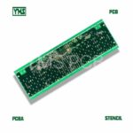
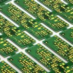
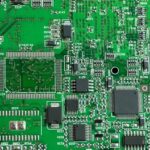
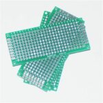
A semiconductor Printed Circuit Board (PCB) refers to a PCB designed to hold semiconductor components like integrated circuits (ICs), transistors, diodes, etc. along with associated passive components. It provides mechanical support, electrical connectivity through copper traces to route signals, and aids heat dissipation for reliable functioning of on-board electronics.
Semiconductor PCBs underpin miniaturized electronic devices we extensively use in computing, communications, consumer, automotive, industrial equipment and more. This article covers details on their construction, characteristics, classifications, design considerations and role in electronics manufacturing.
Key Characteristics of Semiconductor PCBs

Below are some of the typical attributes of a PCB meant for deploying semiconductor components:
Board Materials
- Typically FR4 grade glass-reinforced epoxy laminate material
- Also more advanced substrates like Isola, Arlon etc.
- Selection depends on operating frequencies, power levels, cost targets etc.
Conductive Layers
- Copper foil (1oz / 2 oz generally)
- Layer counts 2 to 32+ to accommodate complex circuit routing
Board Dimensions
- Varies widely – SBCs to HPCBs.
- Dense component mounting trends towards compact PCB sizes
Board Thickness
- Typically 1.6 mm but high layer counts can be thicker ~2.4 mm
- Thinner profiles preferred for portability
Common Components Mounted
- Integrated circuits – MCUs, Controllers, Interface chips, Memories
- Discrete active devices – MOSFETs, Transistors, Diodes
- Passive devices – resistors, capacitors, inductors etc
Fine Pitch Interconnects
- High density BGA, QFP, QFN packages with 0.4 mm to 0.65 mm pin pitches
- Driven by integrated circuit pad dimensions
High Density Routing
- 6-12 mil trace/space
- Microvias, buried and blind vias
- Often 6-8 routing layers or more required
PCB Classifications Based on Design Complexity
Semiconductor PCBs can be segmented into classes based on routing intricacy driven by onboard component needs:
Class 1 Boards
Easy complexity boards with low component counts and large simplicity suitable for automated assembly.
Typical characteristics:
- Low component counts < 50
- Relaxed trace/space requirements
- 4-6 routing layers
- Minimal vias
- Basic simulation needs
Example applications: Simple analog circuits, Basic lighting electronics
Class 2 Boards
Medium complexities boards with moderate component density, regular outlines, and controlled impedances.
Typical characteristics:
- Moderate component count ~ 100
- 6-8 routing layers
- Fine pitch surface mount parts
- Controlled impedance traces
- Thermal analysis recommended
Example applications: Consumer appliances control electronics, LED system electronics
Class 3 Boards
Highly advanced boards with very dense interconnects, high pin counts, tight tolerances and simulations required.
Typical characteristics:
- High component counts > 150
- Very fine trace/space < 6 mils
- High layer counts >10
- Numerous buries/blind vias
- Extensive SI, PI, thermal analysis
Example applications: Telecommunication systems, High speed data processing products
As semiconductor package complexities rise, PCB designers must elevate design sophistication in tandem.
Typical Design Process for Semiconductor PCBs

Designing PCBs suited for complex semiconductor parts involves comprehensive electronic and mechanical evaluations across tools:
1. Define Requirements
Formulates scope covering:
- Electrical functionality
- Component selection
- Interfaces and ports
- Applicable standards
- Mechanical characteristics
- Testing criteria etc
2. Create Schematics
Details components interconnections – serves as input for PCB layout design.
3. Execute System Analysis
Simulates design performance covering:
- Signal integrity
- Power integrity
- Electromagnetic emissions
- Thermal profiling
Fine tune architectures.
4. Floorplanning
Outline board layout blueprints considering:
- Component placements
- Multi-layer stackups
- Zone partitions
- Decoupling strategies
Guides physical implementation.
5. Placement
Map components optimizing:
- Density
- Routability
- Signal paths
6. Routing
Connect placed components through routing layers often with auto-routers.
7. Verify Designs
Runs comprehensive validation checks:
- Electrical rule checks
- Timing analysis
- Signal quality
- Power distribution
8. Documentation
Formal data packages covering:
- Schematics
- BOMs
- Layer plots
- Netlists
- Drawings
- Library packs
9. Prototype Build
Fabricate initial test boards for validation before volume production.
With chip integration complexities rising, semiconductor PCB designs mandate rigorous analysis, verification and prototype testing.
Semiconductor Package Evolution Driving PCB Complexities

The relentless drive towards packing greater functionalities within integrated circuits is raising PCB design and material enhancements imperative for supporting latest semiconductor technologies:
Printed Circuit Board Complexity Progression
As depicted above, PCB stackups, layer counts, trace dimensions and analysis depth continues rising in response to IC integration advancements across technology nodes even as dimensions shrink.
Key Semiconductor Package Categories
IC packing approaches impart unique considerations influencing PCB implementation complexity concerning power delivery, signal routing, shielding etc. apart from pin-density.
PCB Design and Material Considerations
| Component Type | Key Drivers | Design Priorities |
|---|---|---|
| Integrated Circuits | More gates per chip | Signal integrity Power integrity Thermal dissipation |
| DRAM | Higher memory density | Signal quality Multi-layer routing Decoupling |
| GPUs | Faster computational throughput | Ultra high-speed designs EMI containment Vibration resilience |
| FPGAs | Reconfigurable gates | Adaptive routing topologies Tuneable power delivery |
| RF Modules | Higher frequency operations | Controlled impedance Low loss substrates Shielding |
Surging pin counts, densities, frequencies and power needs associated with advancing semiconductor technologies compel enhancements across PCB materials, stackups and design practices for interoperability.
Role of PCBs in Electronics Manufacturing
Printed circuit boards with soldered electronic components bridge the crucial gap between semiconductor devices and finished electronic products with intended functionalities.
Key roles played:
Integrates Components Securely
PCBs utilize epoxy resin boards with layered copper foils to integrate both active ICs and passive discrete devices. SMT assembly solders components reliably onto pads.
Establishes Interconnections
Conductive tracks on multilayer PCBs create wired signal links between attached components pins facilitating flow of power, inputs/outputs and data.
Provides Mechanical Stability
The rigid board physically secures tiny components while withstanding vibration, shocks and impacts through product lifecycles. Greater resilience demanded of mobile devices.
Enables Heat Dissipation
PCBs flats surfaces, exposure and conductive layers promote conduction cooling while thermal vias channel heat from hot components preventing reliability risks.
Supports Testing
Test points designed on boards aids validation of functioning modules supporting fault isolation and repairs.
Allows Encasement
Robust board structures handle protective enclosures, gaskets, coverings etc. tailored across consumer, industrial or military grade environment needs.
For most electronics, PCBs transform loosely integrated tiny semiconductors, passives and other devices into unified building blocks ready for application deployment.
Future Outlook on Semiconductor PCB Advancements

Evolving semiconductor integration complexities will compel PCB material and design innovations on multiple fronts:
Component Miniaturization
- Continual IC geometry shrinking beyond 3nm nodes
- Higher pad densities below 0.4 mm pitch
- Miniaturized passives
Implications: Demands denser routing, thin cores with microvias
Higher Frequencies
- 5G communication above 90 GHz spectrum
- Faster signal modulation rates
Implications: Material characteristic impedance control vital
Power Hungry Components
- Ever rising transistor budgets > 50 billion per chip
- Expanding power appetite > 250W
- Complex voltage planes
Implications: Thicker copper layers, analysis mandatory
Advanced Packaging
- 2.5D, 3D, SiP, chiplets
- Heterogenous integration
- New interconnect types
Implications: Innovative embedding, thermal considerations
While semiconductor advances continue, associated PCB technologies race to enable uncompromised integration.
Frequently Asked Questions
Q1. Why are PCBs crucial for semiconductor devices deployment?
PCBs transform loose ICs and discretes into sturdy electrical circuit assemblies besides enabling connectivity, cooling and protection. Their solid structure durably withstands mechanical stresses from movement, use or environments.
Q2. What are some key PCB substrate materials used today?
FR4 remains ubiquitously popular for cost efficiencies leveraging woven fiber and epoxy resin construction. High frequency designs employ advanced dielectric materials like Isola, Arlon etc. Ceramic substrates used for demanding high power modules.
Q3. What construction enables high density PCB routing?
Very fine trace widths (~5 mils) paired with microvias (~6 mils) and multiple routing layers (16+) allows routing complex semiconductor ICs up to 2500 pins or pads. Careful stackup planning critical.
Q4. Why is SI/PI analysis mandatory for semiconductor PCBs today?
With ICs operating above 3 GHz clocks today and voltages under 1V, vigilant signal and power integrity assessments via simulations during PCB design ensures stable functioning sans signal losses or electrical noise issues.
Q5. How are upcoming embedded component technologies impacting PCB designs?
Embedding passives or actives directly onto boards using printed polymer materials or cavities aim bypassing space constraints but requires design adjustments for electrical, thermal and structural reliabilities.
