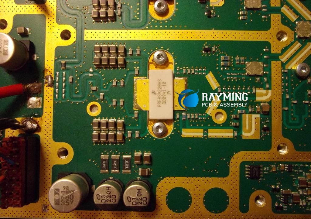
Radio frequency (RF) printed circuit boards (PCBs) are becoming ubiquitous across industries as wireless connectivity gets integrated into products like smartphones, vehicles, IoT devices, communication infrastructure and so on. However, RF design practices have remained a “dark art” relegated to specialized roles.
This article attempts to bridge the gap by introducing essential RF PCB concepts digital engineers should incorporate during board design and layout to avoid common mistakes that degrade signal quality. Following industry-standard methodologies will also help articulate requirements when outsourcing fabrication to vendors.
Signal Integrity Basics
Maintaining signal integrity from chip to antenna is crucial for reliable RF PCB performance. Here are some key factors:
Impedance Control
Impedance indicates effective signal transmission along a conductive path by balancing resistance (R) and reactance (X) components:
Z = R + jX ohms (j as imaginary component)
Matching the impedance of traces to that of components (like 50 ohms) using controlled dimensions minimizes losses as signals propagate through the interface mediums due to electrical length differences.
Insertion Loss
Insertion loss represents signal attenuation as RF energy gets converted into heat over trace lengths. Several improvements are essential:
- Choose materials with consistent dielectric properties over operating frequency ranges
- Minimize number of lamination layers that signals traverse through
- Use thicker metal cladding of 2 oz./sq.ft or above to reduce conductor losses
Crosstalk Prevention
Intended RF signals can couple into adjacent traces causing interference. Mitigation options involve:
- Increase spacing between traces linked to different RF nodes
- Place ground fills or grounded metal barriers between trace clusters
Phase Noise Control
Unwanted fluctuations in signal phase and frequency (noise sidebands) should be analyzed especially for synthesizer and clock routing carrying precise timing signals across baseband and RF interfaces.
Stackup Configuration
The cross-sectional board layer stack determines functionality partitioning across power delivery, shielding, signal control, and thermal management:
Here are some key guidelines:
- Place ground planes next to signal layers for controlled impedance
- Distribute power and ground planes evenly through the stackup
- Assign dedicated power and ground filtering sections
- Incorporate thermal reliefs and heat spreaders if needed
Signal Routing
Applying constraints related to placement, orientation and geometry during routing is vital:
Some proven techniques involve:
- Use 45o/90o bends for direction changes rather than arcs
- Avoid T-junction or pi-type splits; use arc or tapered geometries
- Make trace widths slightly thicker than stripline gap
- Add teardrop anchors at SMA pads to reduce stresses
Shielding
Shielding prevents external interferences from disrupting sensitive RF nodes:
Approaches range from:
- Fencing signal areas with ground copper
- Creating compartmentalized boxes with metal and plating via fences
- Using on-board covers with spring contacts or gaskets
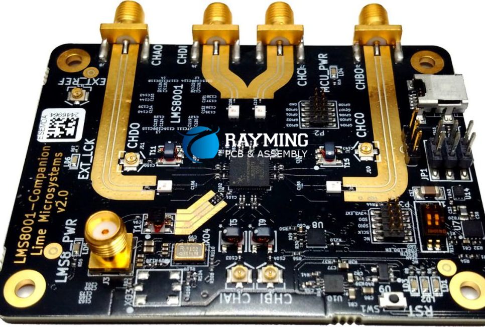
Antenna Integration
Seamlessly integrating antennas, matching their impedance and steering radiation patterns are crucial:
- Minimize transmission line length from IC to antenna feed
- Place baluns for balanced-to-unbalanced signal conversion
- Model far-field radiation patterns using simulation
Material Selection
Substrate properties like dielectric constant (Dk) and loss tangent directly influence RF signal propagation. Some options:
| Material | Dk | Loss Tangent | Key Attributes |
|---|---|---|---|
| PTFE | 2.2 | 0.001 | Lowest loss; expensive |
| FR-4 | 4.3 | 0.025 | Low cost; higher loss |
| Rogers RO4000 | 3.38 | 0.0027 | Stable electrical properties |
| Taconic RF-35 | 3.5 | 0.0018 | Hybrid PTFE ceramic filler |
| LCP | 3 | 0.002 | Excellent signal quality up to mmWave bands |
Table 1: Substrate materials comparison for RF PCBs
Additionally, thermoset laminates provide better environmental resistance while thermoplastics enable superior heat dissipation.
Design for Manufacturing

Keep these DFM tips in mind during layout:
- Use rectangular keepout zones for vias and traces needing tight impedance control
- Incorporate thermal reliefs, corner chamfers and rounded pad shapes
- Define test points, probe pads and fixtures for post-assembly RF measurements
- Request fabricators to share stackup drawings, material certifications and test procedures upfront
Developing close partnerships with manufacturers through design reviews is key to realizing optimal fabrication yields.
Simulation and Analysis
Running signal, thermal and mechanical simulations using tools like Ansys HFSS, Keysight ADS, Cadence Sigrity, Mentor HyperLynx minimizes potential flaws before committing expensive RF PCB prototypes for testing:
DOE (design of experiments) techniques help evaluate stackup alternatives efficiently. Simulation model exchange using standards like ODB++ enables tighter ECAD-MCAD collaborations.
Testing and Characterization
Electrical compliance testing and inspection procedures required for RF PCBs from fabrication through end-use application stages:
These range from:
- Destructive microsectioning for interface quality checks
- Microwave impedance measurements to validate material properties
- S-parameter evaluations using VNA for insertion/reflection loss analysis
- Highly accelerated stress screens (HASS) for product reliability validation
Getting Certified with IPC Standards
IPC, the electronics industry association, has defined verification criteria through acceptance standards like IPC 6018, 60068 and various J-STD Class 3 workmanship guiding documents.
Becoming familiar with quality management system processes, achieving certification and requiring your manufacturing partners to do so ensures meeting regulatory compliance needs of end-use industry segments like defense, aerospace, automotive etc.
Frequently Asked Questions
Q1. Why are 90-degree bends preferred over arc shapes during RF trace routing?
A1. Right-angle trace bends provide consistent impedance control compared to variable impedance in arching curves that act as natural antennas emitting energy non-uniformly – reducing transmission efficiency.
Q2. What are thermal reliefs in PCB context?
A2. Thermal reliefs refer to adding thin traces or voids between pad connections to prevent solder cracks from propagating inside due to coefficient of thermal expansion (CTE) mismatches between assembly materials upon temperature fluctuations.
Q3. How are RFMeasurements for insertion loss or return loss conducted?
A3. Using a Vector Network Analyzer (VNA), S-parameter measurements are done by connecting test ports to a calibration substrate like GGB Industries’ CSR-8 kit to characterize losses across transmission lines over desired frequency ranges from 30 MHz to 70+ GHz.
Q4. What are common RF PCB defects needing inspection?
A4. Some examples include insufficiently filled vias causing opens or shorts, inconsistent dielectric spacing between layers leading to variable impedance, surface roughness degrading skin effect performance and inadequate peel strengths that cause delamination.
Q5. How can digital engineers upskill for RF PCB design jobs?
A5. Getting familiar with signal propagation, antenna and wireless communication basics through online courses combined with learning EMI/EMC standards plus hands-on experience using modeling tools like Ansys HFSS or Keysight ADS is a great way to start transitioning careers.


