Printed circuit board (PCB) layout involves taking the schematics of an electronic circuit and converting it into the physical layout artwork containing component footprints, copper tracking, pads, vias and other geometric features. This layout artwork is used for fabricating the actual PCB prototypes and production units. PCB layout services refer to outsourcing the layout design process to an expert PCB layout company to create the fabrication-ready layout files as per the client’s design requirements. This article provides a detailed overview of PCB layout design services – their benefits, the layout process, factors to consider when choosing a service provider, key technologies, and more.
What are PCB Layout Services?
PCB layout services allow OEMs (original equipment manufacturers) and design engineers to outsource the complex and specialized task of converting schematics or HDL code into a finished PCB layout that is ready for fabrication and assembly.
The client provides the logical design data – schematics, bill of materials, component library, design rules etc. The layout services partner then translates this into the physical board layout by executing tasks such as:
- Placement of components on the board
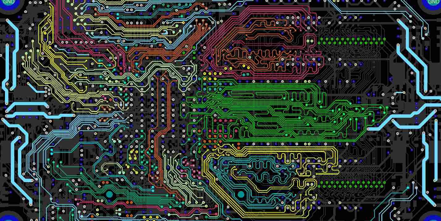
- Routing copper tracks between pads
- Assigning net names
- Specifying stackup layers
- Defining board outline and mechanical features
- Adding essential text like reference designators
- Checking electrical and physical rules
- Generating fabrication and assembly drawings
- Validating manufacturability
The final deliverable is a comprehensive set of layout files and drawings ready to be sent to a PCB manufacturer for fabrication and assembly. This can accelerate product development by letting designers focus on design engineering rather than board layout.
Benefits of Using PCB Layout Services
The many benefits of outsourcing layout design rather than attempting in-house layout are:
Fast Turnaround
- No need to train internal layout engineers. Quick start of layout work.
Cost Savings
- Eliminates fixed employment costs. Reduces tool costs.
Experienced Engineers
- Access to layout experts with knowledge of latest tools and technologies.
Quality and Reliability
- Mature processes used by the service provider result in robust, fabrication-friendly layouts.
Design Rule Checking
- Service providers can validate complex electrical and physical constraints.
Reduced Workload
- Frees up internal engineering time to focus on core design.
Flexibility
- Easy to scale work up and down based on changing requirements.
Multi-CAD Support
- Service providers have expertise in using a variety of EDA tools.
Prototyping Support
- Layouts optimized for fast fabrication of engineering prototypes.
Manufacturing Support
- Assistance with fabrication and assembly drawing generation.
For most small and medium companies, outsourcing PCB layout offers huge advantages in productivity, time-to-market and cost control. Large organizations may use a mix of internal layout and external support.
PCB Layout Design Stages
The typical printed circuit board layout design process involves the following key stages:
1. Design Data Collection
The client provides the required inputs for layout design – schematics, bill of materials, component datasheets, board outline dimensions, placement directives, design rules, layer stackup, fabrication notes etc.
2. Design Review and Analysis
The PCB layout engineer studies the schematics to understand circuit connectivity and analyses the BOM and datasheets to determine placement, routing and thermal considerations. Preliminary stackup, layer counts and design rules are defined.
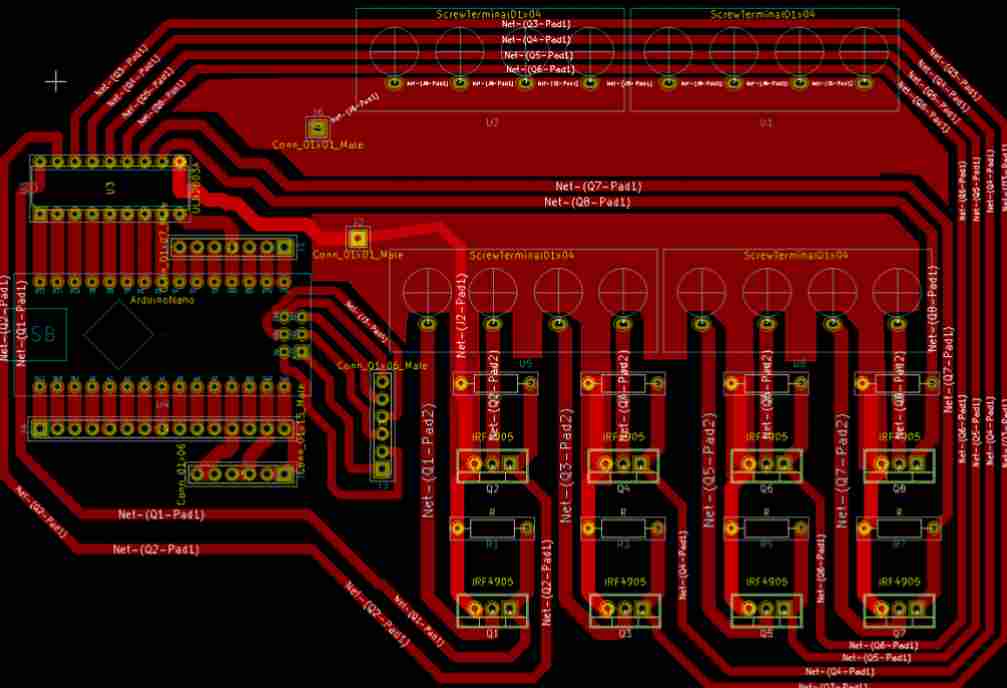
3. Component Placement
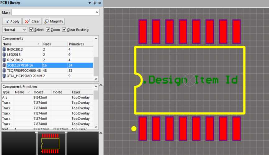
Electrical and electronic components are arranged on the board according to schematics, layout guidelines, routing needs, and manufacturing preferences. Often done interactively using PCB layout software.
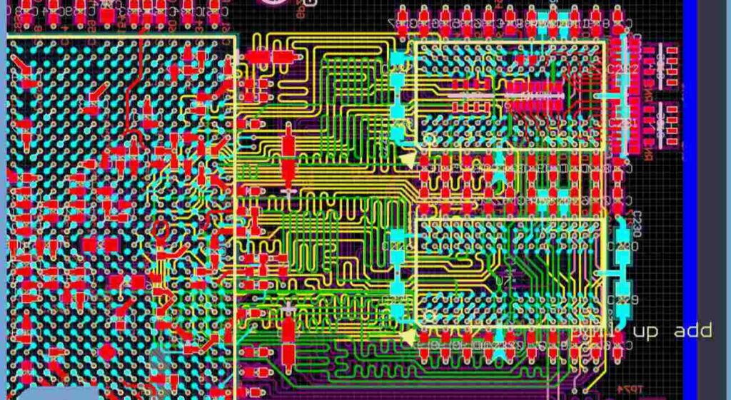
4. Component Routing
Electrical connectivity signals between placed components are routed on appropriate layers using copper tracks and vias following electrical and physical constraints. Done manually or interactively.
5. Design Rule Checking
Electrical rules like nets, classes and constraints are defined. The layout is verified against constraints like spacings, widths, drill sizes, etc. Errors are corrected.
6. Manufacturing Output Generation
Drawings, fabrication and assembly notes, layer plots, drill tables, netlists, BOMs, component centroid data, and other outputs are generated.
7. Design Validation and Review
The client reviews the fully routed layout for correctness as per schematics and HW design intent. Errors are fixed in an iterative process until sign-off.
8. Final Manufacturing Data
After sign-off, the fabrication and assembly data is finalized. Gerber, NC drill, pick-and-place, assembly drawings etc. are sent to the client for board fabrication and assembly.
Here is a quick video overview of the PCB layout design process:
PCB Layout Design Process Video
This well-defined, step-by-step layout process ensures an efficient handoff from schematics to fabrication-ready layout while meeting all electrical and physical design constraints.
Choosing a PCB Layout Services Provider
When selecting an external PCB layout partner, OEMs and design firms should evaluate the following key aspects:
Technical Expertise
- Depth and breadth of layout experience
- Familiarity with latest layout tools and emerging technologies like HDI, rigid-flex, embedded passives etc.
- Skill in schematic capture, component library creation etc.
- Specializations like RF/microwave, digital, analog, power electronics etc.
Quality Processes
- Use of version control and change management systems
- Design rule checking and verification procedures
- Configuration management and data security
- Quality certifications like ISO 9001
Tool Proficiency
- Expertise in major layout EDA tools like Altium, Cadence, Mentor, Zuken etc.
- Ability to handle data from diverse design environments
Program Management
- Account management structure for customer coordination
- Ability to provide 24/7 engineering support
- Order tracking and progress visibility
Capacity Scalability
- Infrastructure and staff to flexibly adjust to changing demand
- Ability to take on additional work at short notice
Cost Structure
- Pricing model – fixed bid or time & material
- Minimum order values
- Discounts on high volumes
IP Protection
- Non-disclosure agreements to protect proprietary customer data
- Secure data management practices
Evaluating PCB layout partners on these parameters helps identify the right provider who can deliver a high-quality, fabrication-ready layout in the shortest possible time.
Key Technologies Used in PCB Layout
Modern PCB layout leverages a variety of software tools and emerging technologies for addressing complex design challenges. Some key ones are:
EDA Tools
Advanced PCB layout is done using electronic design automation (EDA) software suites like Altium Designer, Cadence Allegro, Mentor Xpedition, Zuken CR-8000 etc. They integrate schematic capture, layout, autorouting, design rule checks and manufacturing outputs. Many also offer 3D visualization.
Design for Manufacturing
DFM practices like component placement, trace geometries, test points, tooling holes etc. are designed keeping PCB fabrication and assembly processes in mind. This avoids manufacturing issues and minimizes prototyping iterations.
HDI Technologies
To support high density interconnect PCBs, layout leverages technologies like microvias, blind/buried vias, thinner dielectrics, tighter tolerances, controlled impedance tracks etc.
Embedded Passives
Embedding capacitors, resistors and other passives into the PCB itself saves space and cost. Layout provides for designer-controlled cavities and pad geometries to enable this.
Rigid-Flex
Flexible PCB sections enable three-dimensional packaging while maintaining reliability. The layout incorporates special features for flex-to-rigid interfaces and dynamic flexing zones.
Signal Integrity
Signal integrity is ensured by matching trace geometries, assigning return paths, controlling impedance, minimizing stubs etc. at the layout stage. SI/PI simulations validate performance prior to fabrication.
Thermal Modeling
Thermal analyses help determine optimum component placement to avoid hotspots under peak heating conditions. Thermal vias, polygons, thermal pads aid cooling.
By embracing these and other technologies, PCB layout services are able to handle the increasing design complexity driven by products requiring advanced functionality in highly compact form factors.
Conclusion

In summary, PCB layout services provide many advantages to companies looking to shorten development cycles and optimize costs for bringing new electronic products to market. Selecting an expert layout services partner allows designers and engineers to focus their efforts on product innovation rather than get bogged down in layout implementation details.
With capabilities like multi-CAD support, familiarity with emerging layout technologies, robust quality systems and polished program management, the right service provider delivers fabrication-ready layouts that meet the most demanding design rules and performance criteria. By leveraging such services strategically, OEMs can gain dramatic improvements in engineering productivity and faster time-to-market. As electronics design complexity increases, PCB layout services become an even more valuable resource.
FAQ
Here are some frequently asked questions about PCB layout services:
Q1. When should I consider outsourcing vs. doing layout design internally?
For low to medium complexity designs without specialized requirements, internal layout may be suitable. But for high density designs, HDI, RF/microwave, miniaturization etc. external expertise is preferable. Outsourcing also helps when internal bandwidth is constrained.
Q2. How can I safeguard my IP when using a third-party layout service?
Reputable layout providers use secured data systems and non-disclosure agreements to protect customer IP. They usually work with numerous clients simultaneously and have robust data segregation practices.
Q3. What data does the layout partner need from me to start the layout work?
To initiate layout design, the service provider needs schematics, bill of materials, component library, board dimensions, placement directives, layer stackup, design rules and other specifications.
Q4. Does using layout services increase the risk of errors in my design?
No, a good layout partner has qualified staff and rigorous design review and verification processes to detect errors early. Responsibility for electrical correctness remains with the designer. The service provider focuses on physical implementation.
Q5. How can layout services help me in prototype and low volume manufacturing?
The service provider can support you with manufacturing documentation like assembly drawings, fabrication notes, test point markings, stencil and jig design etc. specifically tailored for prototype builds and small scale production.


