The PS5 gaming console from Sony packs tremendous processing capabilities enabling immersive experiences and lightning fast performance. Powering the core of the system lies a meticulously engineered printed circuit board (PCB) integrating cutting-edge silicon, interfacing, and power regulation technologies.
This article will provide an overview of the PS5 PCB. We’ll explore key components mounted on the boards, analyze the PCB layout considerations, and discuss manufacturing approaches for these complex modules. Learning the principles behind the PS5 PCB gives insights into state-of-the-art consumer electronics development.
PS5 Hardware Architecture Overview
First, let’s ground the overarching system block diagram showcasing sub-systems facilitated by the central PCB:
PS5 Architectural Overview
We see the PCB interlinks core computing, graphics, memory, storage, connectivity, user interfaces, power and thermal management across a sophisticated platform.
Key Characteristics
Drilling into specifics, the PS5 PCB carries critical performance mandates:
PS5 PCB Attributes
- Multi-substrate stacked pair
- Digital logic & power regulation
- 16+ layer construction
- Signal routing density
- High speed differential interfaces
- Multi-GHz signaling
- Low-inductance optimized power
- Supply transient integrity
- Thermal co-design focus
- Heat dissipation spreaders
- Complex subsystem partitioning
- Managing crosstalk risks
These targets push manufacturing capabilities requiring advanced PCB technology integration by Sony’s developers.
Component Population Analysis
Driving so much system functionality requires populating a vast array of advanced components:
PS5 PCB Part Classes
| Part Class | Purpose | Key Examples |
|---|---|---|
| Processor | Game compute engines | AMD Zen SoCs |
| Memory | Data storage | GDDR6 SDRAM |
| Storage | Game asset repository | Custom SSD solutions |
| I/O Interfaces | External connectivity | USB4 controllers |
| A/V Components | Graphics display data | HDM/DP conversion ICs |
| Clock Generation | Synchronization timing | Differential signal PLLs |
| Power Regulation | Supply rail generation | Multiphase buck converters |
| EMI Suppression | AC line filtering | Common mode chokes |
| Thermal Interface | Cooling enhancement | Gap pad material |
| Passive Integration | Power rail decoupling | Multilayer ceramic caps |
| Other Support | Specialty assist ICs | Real time controllers |
This diversity covers the entire system gamut from data processing out to end user interactions.
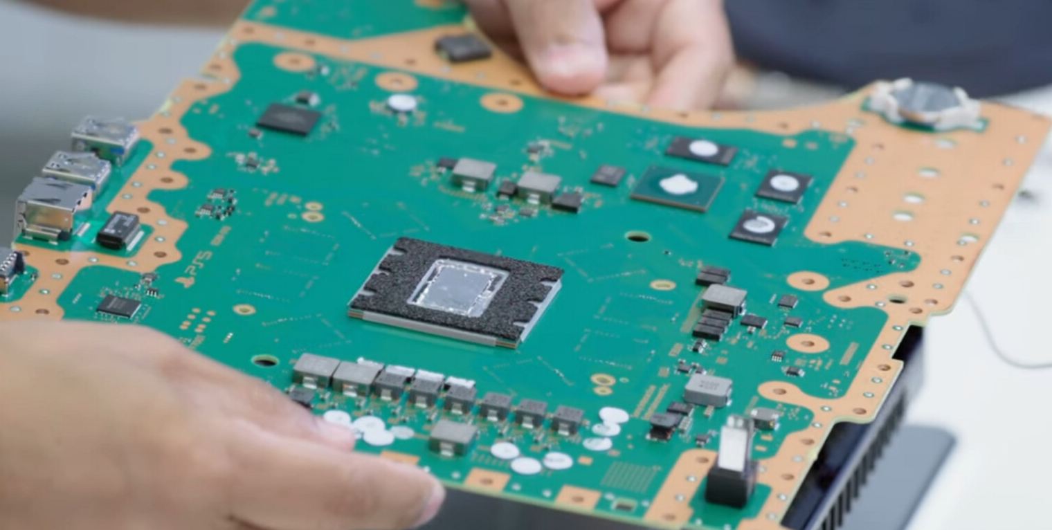
Core Processor Integration
While many components populate the PCB, analyzing just the principal processor integration proves instructional:
PlayStation 5 SoC
- 7nm AMD Ryzen “Zen 2” chiplet
- 8 core, 16 thread CPU
- Soldered BGA package
- Integrated Radeon GPU
- 36 compute units
- 48-50GHz operation
- 256-bit bus interface
- 16GB GDDR6 SDRAM
- 14Gbps speed grade
- Custom unified memory approach
- Surrounding power stage integration
- Over 200 pins for power/ground
- Processor package substrate
- Redistributes ~2000 I/O to solder balls
- Low inductance socketing
- Minimize transient noise pickup
- Local supply decoupling
- Supports fast dynamic loads
This example highlights the engineering efforts involved in just the key computing components alone, with equal diligence required on all supporting elements of the complete multi-layer PCB stackup.
Key Layout Considerations
Translating the architecture into physical implementation on the PCB demands advanced planning:
PS5 PCB Design Focus Areas
| Consideration | Details |
|---|---|
| Signal Escape Routing | Breaking out high pin count BGA leads |
| Multi-GHz Traces | Controlling matched length lines |
| Channel-to-Channel Isolation | Managing crosstalk noise |
| Surface Mount Attach | Solder process integrity |
| Via Structures | Handling return current flows |
| Controlled Impedances | Minimize transmission line reflections |
| Stackup Formulation | Balance signal layers and power planes |
| Component Keepouts | Satisfy safety agency spacing rules |
The Schematic-to-Layout handoff requires extensive upfront modeling to achieve performance targets under practical manufacturing constraints.
PCB Substrate Attributes
Realizing the PCB itself involves specialized material selection:
PS5 PCB Stackup
| Layer Class | Implementation Notes |
|---|---|
| Dielectric Materials | High performance polymers enable thinner cores for lamination layer counts |
| Conductive Layers | 1⁄2 oz and 1 oz copper foils balance throughput needs and fine pitch capabilities |
| Finish | Surface treatments like ENIG (Electroless Nickel Immersion Gold) provide durability and interconnect integrity |
| Solder Mask | Tight tolerance SMT registration supports mounting fine pitch components |
| Silkscreen | Tight tolerance component labeling and identification |
| Via Structures | Staggered patterns prevent via-to-via coupling – key for multi-GHz signals |
| Edge Connectors | Board-to-board connectors facilitate midplane stacking |
These PCB attributes help satisfy specialized electrical, mechanical, and thermal requirements in the console.
Manufacturability Considerations
In realizing the PS5 PCB, Sony partnered with leading fabricators driving tightly controlled processes:
Fabrication highlights
- Validation of supplier capability
- 16+ layer constructions
- Fractional micrometer alignment
- Conformal coatings
- Antistatic insulation
- Water resistance
- Extensive test coverage
- Bed-of-nails electrical
- ICT fixtureless in-circuit
- Flying probe analog signature analysis
- X-ray layer imaging
- Test coverage automation
- Rigorous quality management
- Source inspection of materials
- Process monitoring
- Traceability practices
These diligent fabrication measures ensure reliability and performance validation success across the product’s operational lifetime.
Thermal Design Analysis
With massive compute power comes substantial heat generation that thermal design directly addresses:
Thermal Planning
- Professor GPU and surrounding memories
- Constitute primary hotspots
- Multi-substrate partitioning
- Separates ground planes
- Strategic cutouts
- Prevent lateral heat spread
- Aligned cooling interface
- Optimized sink mounting
- Nearby sensor integration
- Closed loop fan driving
Extensive thermal simulation and testing ensures the PCB design adequately dissipates the heat fluxes involved.
Signal Integrity Considerations
Routing multi-GHz traces over practical manufacturing constraints involves thorough pre-layout analysis to ensure signal integrity:
High Speed Design Study
- Cross-sectional EM simulations
- Refine line geometry
- Top layer microstrip lines
- Controlled impedance
- Matched length tuning
- Isolate skew
- Breakout optimization
- Smooth layer transitions
- Differential pairs
- Reduce EMI emissions
- Extensive power fill
- Minimize ground noise
- Layer reserving
- Simplify flow planning
First-pass success at multi-GHz speeds necessitates exhaustive virtual modeling before implementation to reduce risk.
Design Tooling
To provide the layout execution capabilities demanded in such an advanced PCB requires leading-edge software toolchains:
EDA Technology Leveraged
- Mentor Graphics Xpedition
- Enterprise-level PCB layout
- Mentor Valor NPI
- Manufacturing prep automation
- Synopsys HSPICE
- Gold-standard circuit simulation
- Ansys HFSS
- 3D EM field solving
- Altium
- Unified design platform
- MATLAB
- Modeling & analysis programming
These world-class solutions enable handling the immense complexity involved in architecting and routing the PS5 PCB substrate while ensuring manufacturability.
Frequently Asked Questions
What is the actual size of the PS5 PCB?
Measuring approximately 390mm x 104mm, the PS5 PCB provides extensive real estate to distribute the various controllers and logic around the perimeter with processors, memories and converters occupying the full span.
How was component selection and qualification performed?
Sony engineers applied stringent supplier screening measures on parameters like manufacturing consistency, extended longevity testing, and conformance to specification tolerances like IPC-6012 Qualification and Performance addendums.
What standing technical challenges remain in PS5-class PCBs?
Engineers continue pushing against bottlenecks in high-density component mounting, interfacing heat removal structures, modeling signal losses, and optimizing number of layers required against practical fabrication yields.
What PCB testing strategies validated performance?
In addition to basic structural tests, engineered system-level


