Solid State Drives (SSDs) have become the primary storage medium across consumer laptops to enterprise data centers. Unlike conventional Hard Disk Drives (HDDs), SSDs utilize printed circuit board (PCB) technology to mount solid state flash memory chips along with controller and interface components in a ruggedized enclosure.
This article provides an overview of PCBs designed specifically for SSD cards or modules. We analyze key characteristics, architecture considerations and evolving trends in SSD PCB technology.
Contents:
- Role of PCBs in SSD Products
- SSD PCB Design Complexities
- Architecture Comparison
- Emerging Innovations
- Application Impact
- Conclusion
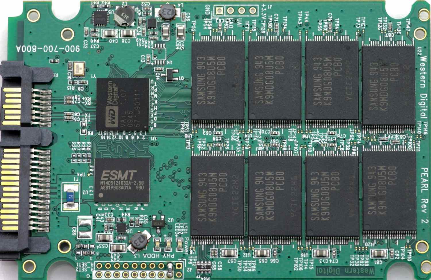
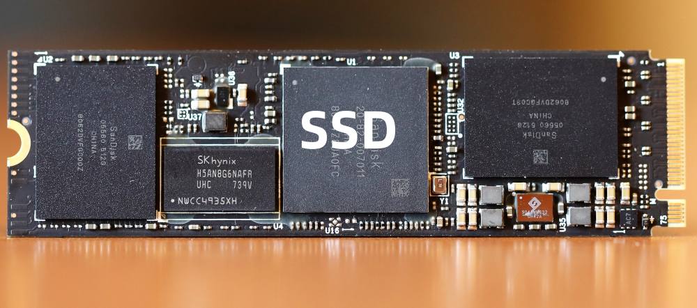
Role of PCBs in SSD Products
Printed circuit boards (PCBs) serve as the foundation platform interconnecting all storage sub-systems within solid state drives including:
- NAND flash memory to store data
- Controller enabling memory access
- DRAM buffer for caching
- Host side connector/cables providing drive interface
- Power circuitry distributing clean power
- Additional components like capacitors; LEDs etc.
The PCB offers mechanical stability for mounting heat sinks over controllers, connectors and facilitates efficient routing for high speed data signals across SSD cards. Intricate PCB layout is vital for contemporary SSD speeds upto 10x faster than old HDDs.
Next we discuss key PCB design intricacies demanded by high performance SSDs.
SSD PCB Design Complexities

SSD PCB layouts deal with substantial complexities around:
Signal Integrity – High speed multi-gigabit SerDes channels prone to losses demand precise impedance control, layer stack-up and routing tactics.
Thermal Management – Controller, DRAM and NAND flash heat density requires sufficient thermal transfer through copper layers, thermal pads and heating sinks mounting.
EMI Containment – Rapid parallel signals necessitate shielding, effective grounding and cross-talk reduction techniques.
Form Factor Constraints – Compact SSD standards like M.2 demand extremely tight PCB component placement and routing.
Reliability Testing – SSD cards undergo wide temp cycling, vibration and bending tests through product lifetime.
Evolving Interfaces – Rapid interface updates like PCIe Gen5, CXL require regular PCB layer stack adjustments.
Component Miniaturization – Continued NAND die shrinks demand modification of placement and layouts.
Let’s analyze popular SSD PCB architectural styles employed.
SSD PCB Architecture Comparison
Two rival architectures have evolved for SSD PCB implementations:
1. Discrete PCB – Separate PCBs for (a) Flash memory (b) Controller and DRAM (c) Connectorintf. Interconnected through interposer boards.
Benefits:
- Modular upgrade
- Independent optimization per function
- Distributed thermal load
2. Integrated Monolithic PCB – Single PCB mounting all sub-systems.
Benefits:
- Miniaturization (single chip scale package)
- Cost efficiency
- Signal/power integrity
Discrete PCB used to be common earlier providing flexibility to upgrade memory. However, space constrained formats like M.2 now popularized integrated monolithic PCB for optimum performance.
We finally highlight latest technology advancements within SSD PCB domain.
Emerging Innovations in SSD PCBs
Major ongoing improvements include:
Heterogenous Integration – Integrate storage class memory options like Intel’s Optane besides NAND using high density substrate or interposer layers.
Advanced Routing Materials – New RF materials like Taconic’s TRF materials implement tightly coupled differential traces to push 25+ Gbps SerDes bandwidth.
Embedded Actives/Passives – Incorporate resistors, capacitors within buildup layers enabling power supply over boards.
Thermal Interface Materials – Advanced thermally conductive substrates substitute FR-4 copper layers for 5x more heat dissipation.
AI Driven Analysis – Leverage predictive analytics to identify resonance risks, EMI hotspots through simulations using ANSYS HFSS, Hyperlynx etc.
Application Impact of Innovations
The cumulative effect of SSD PCB innovations catalyze order-of-magnitude improvements in storage performance across:
Data Centers – Doubled IOPs throughput and density per server rack for Big Data/AI applications
High End Computing – Multi-petabyte shared memory applications
Consumer Devices – Ever lower read-write latencies and lengthened drive durability spanning smartphones to PCs.
Conclusion
In summary, high complexity PCB layout forms the backbone powering rapid enhancements across solid state storage ecosystems. Tight integration of flash memory, controllers, DRAM and interfaces over single advanced PCBs will continue to accelerate SSD speeds and densities over the next decade.
I hope this piece provides useful perspective on the pivotal role of PCB technology enabling contemporary solid state drives. Please share feedback or queries in comments!


