Design
-
Read more: Full Guide – Design Electronics in SnapEDA (Step by Step)
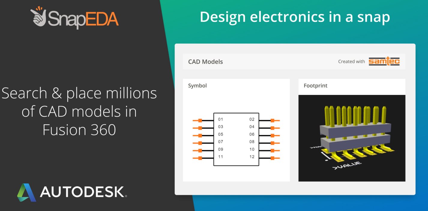
SnapEDA is a free, cloud-based design platform used by electronics engineers to research, design, and collaborate on printed circuit board (PCB) projects in one unified workspace. The SnapEDA Editor tool allows interactively: An integrated component library contains over 500k manufacturer parts covering all needs from single board hobby projects to … Read more
-
 Read more: What Are Solder Pad? ( types, size, spacing, repair and Design tips )
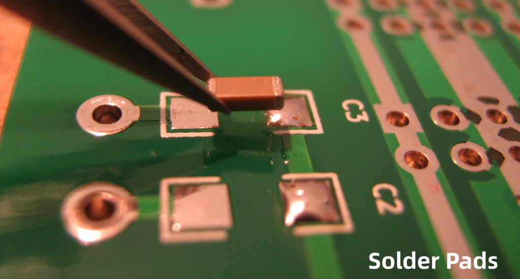
Solder pads constitute one of the most vital elements on a printed circuit board (PCB) facilitating reliable interconnections from components to copper traces during the soldering assembly process. They represent termination points or localized metallized areas on the board providing wettable surfaces for anchoring and forming solder joints with component … Read more
-
 Read more: What is the Difference Between a Microstrip and a Stripline in PCB ?
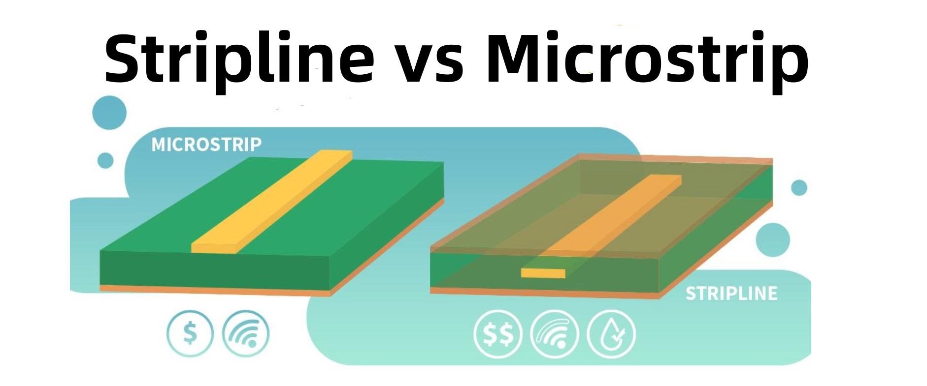
Microstrips and striplines represent common transmission line structures used in PCBs for routing high speed signals. Despite some superficial similarities, these two approaches have important distinctions in terms of construction, characteristics, modeling complexity and usage. We will contrast these transmission line varieties across key factors: Analyzing pros and cons provides … Read more
-
 Read more: Use PCB Teardrops to Increase Yield & Design Quality
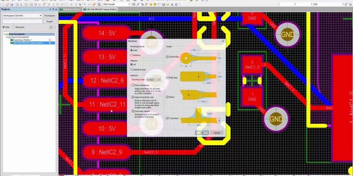
Printed circuit boards (PCBs) form the foundation of electronics products and systems. As PCBs become denser with shrinking feature sizes, maintaining high fabrication yields and reliability requires paying attention to the finer aspects of board layout and design. One such important design technique is the use of teardrops. Teardrops are … Read more
-
How to Design PCB Via Current Capacity ?
Posted by
–
 Read more: How to Design PCB Via Current Capacity ?
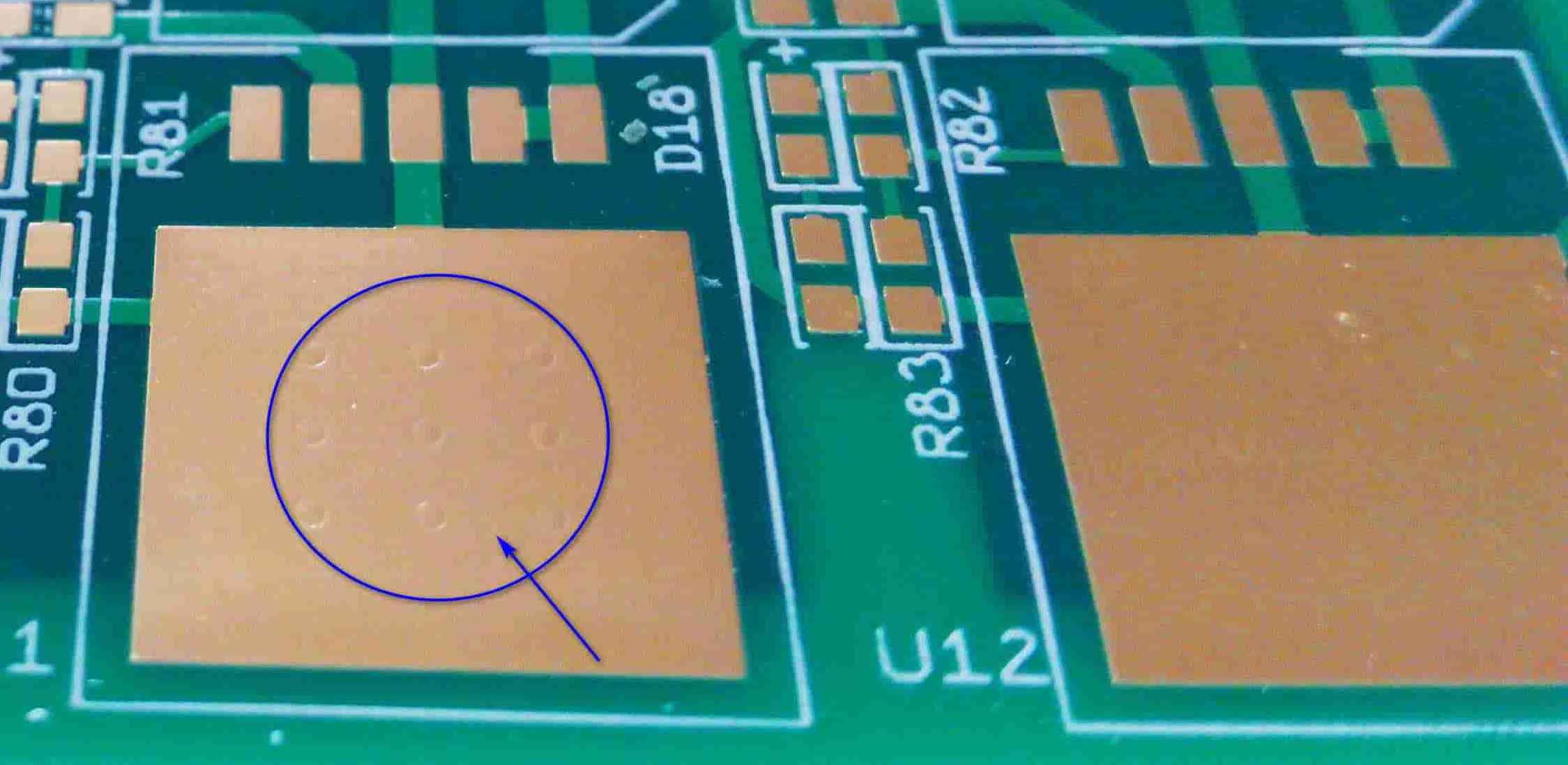
Vias play a critical role in printed circuit boards (PCB) by facilitating interconnections between layers to route signals and distribute power. The current carrying capacity of vias must be adequately designed to ensure power integrity and prevent reliability issues due to overheating. This article provides a comprehensive guide on how … Read more
-
Can You Put a Via in a Pad?
Posted by
–
 Read more: Can You Put a Via in a Pad?
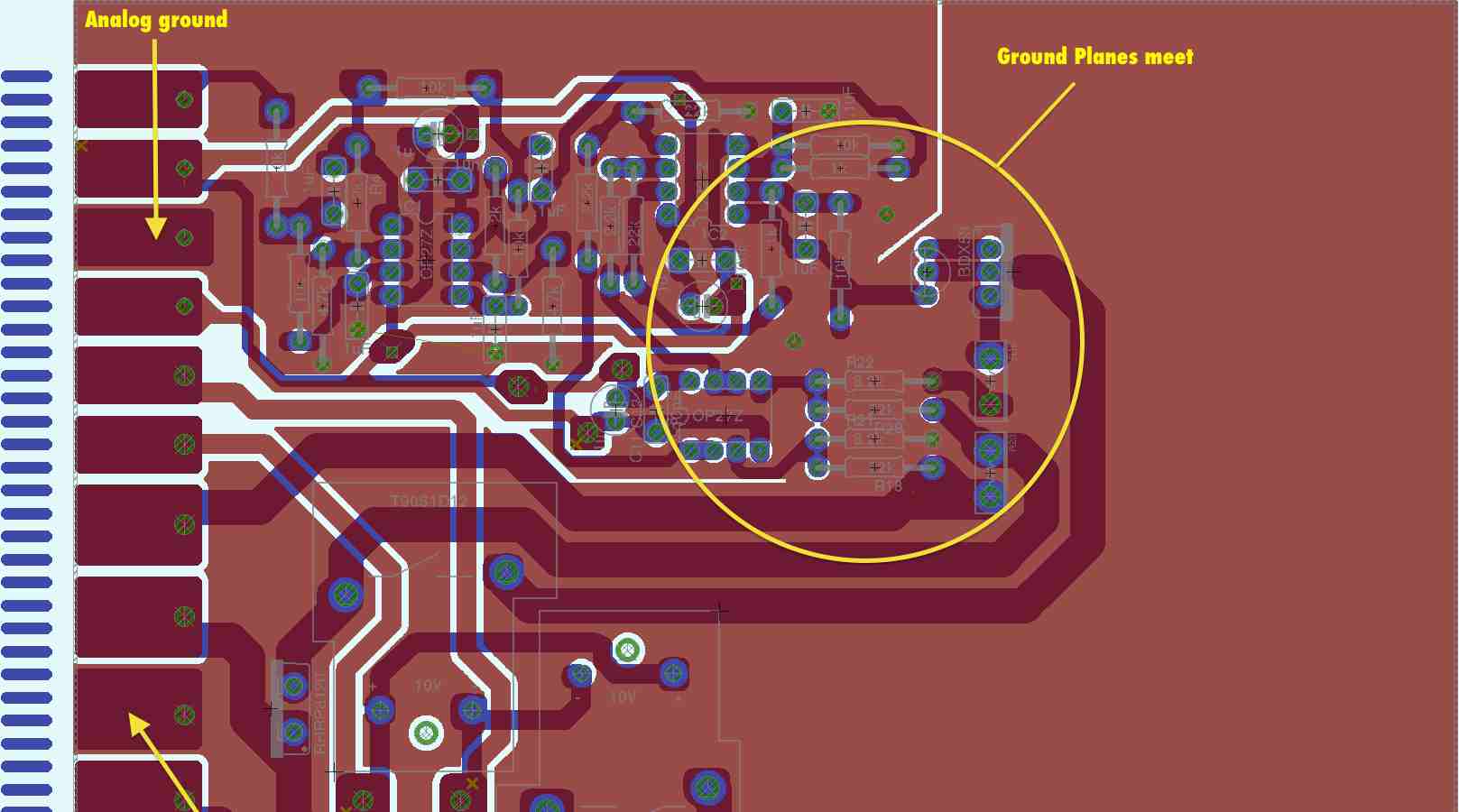
Vias and pads are essential features on printed circuit boards that enable routing connections between layers and mounting components. Vias connect between layers, while pads provide the bonding surfaces for attaching component terminations. At times, pads may need to incorporate vias within them to transfer signals to other layers. But … Read more
-
What Are Gerber Files ?
Posted by
–
 Read more: What Are Gerber Files ?
Gerber files are a standard file format used for Printed Circuit Board (PCB) design and manufacturing. They provide a way to transfer PCB layout data from CAD software to PCB fabrication equipment. Gerber files split the PCB layout into separate layers, allowing each layer, such as copper traces, silkscreen, solder … Read more
-
What is a Ground Loop ?
Posted by
–
 Read more: What is a Ground Loop ?
A ground loop refers to an unintended current flow between two points assumed to be at the same ground potential. Ground loops can arise from improper PCB and electrical design, and can cause a range of issues from noise and signal interference to malfunctions and equipment damage. This article provides … Read more
-
What is the Basic Rule of PCB Layout?
Posted by
–
 Read more: What is the Basic Rule of PCB Layout?
Introduction Printed circuit board (PCB) layout is the art of arranging components and routing connections on a PCB to implement an electronic circuit. While there is significant complexity and specialization in PCB layout, adhering to some fundamental rules and guidelines will help ensure a successful board layout. This article will … Read more
-
What is PCB Layout Services ?
Posted by
–
 Read more: What is PCB Layout Services ?
Printed circuit board (PCB) layout involves taking the schematics of an electronic circuit and converting it into the physical layout artwork containing component footprints, copper tracking, pads, vias and other geometric features. This layout artwork is used for fabricating the actual PCB prototypes and production units. PCB layout services refer … Read more
Recent Posts
- Understanding the PCB Burn-in Testing Process in PCB Manufacturing!

- Unlock the Potential of Embedded PCB Assemblies for Improving the Performance of Electronics Devices

- What are the Advantages of Custom Cable Assembly to meet your bespoke needs?

- What are the benefits and limitations of custom PCB boards?

- What are the benefits of Prototype PCB manufacturing and why is it important?

Categories
- 3D Guides 2,663
- Components 4
- Design 22
- Electronics 20
- PCB 125
- SMT 27
Tag Cloud
There’s no content to show here yet.