A ground loop refers to an unintended current flow between two points assumed to be at the same ground potential. Ground loops can arise from improper PCB and electrical design, and can cause a range of issues from noise and signal interference to malfunctions and equipment damage. This article provides an overview of ground loop concepts, causes, effects, detection and mitigation in PCB design.
What is Ground?
Ground refers to a common return path in an electric circuit from which voltages are measured. Ideal grounds remain at 0V potential and provide a low impedance path return for signals and power.
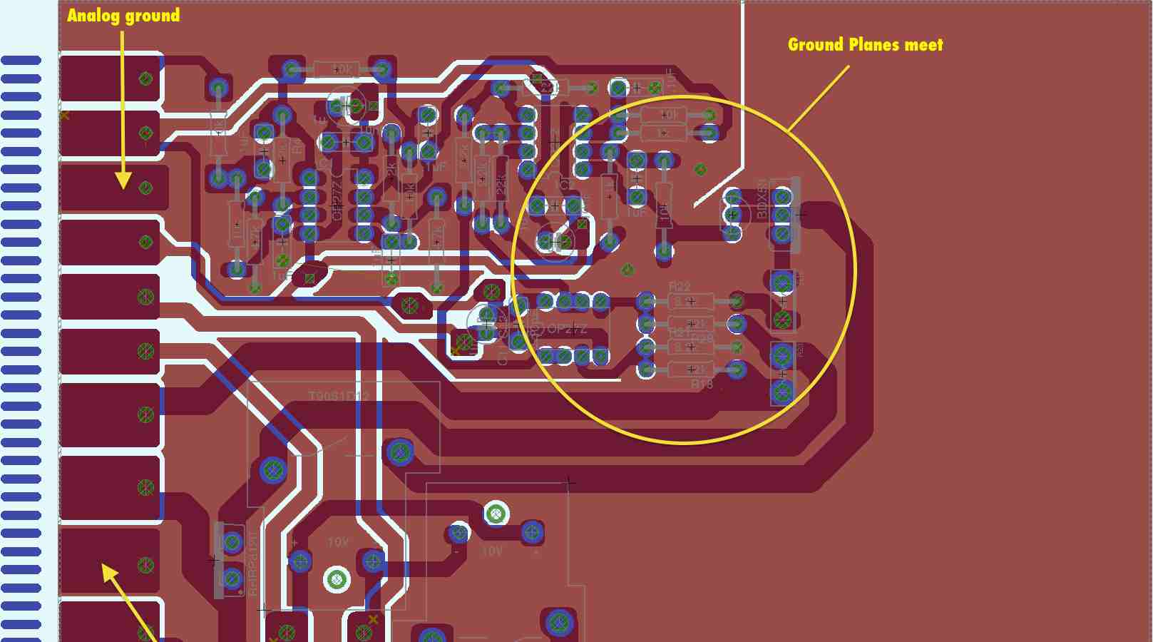
On a PCB, ground typically refers to the copper pour or traces connected to the ground pins of devices, power supplies, and chassis. Multiple ground points are connected to create a common ground plane at reference 0V potential.
This shared ground allows signals to return to a common 0V and provides a sink for return currents in the circuit.
What is a Ground Loop?
A ground loop occurs when there are multiple current return paths between two points assumed to be at the same ground potential. This creates unintended voltage differences and circulating currents between ground points.
For example, if device A and B are grounded at different points, and a wire connects the grounds, then a loop is formed allowing current to flow between the ground points.
This unintended auxiliary current path creates electrical noise and improper grounding operation.
Causes of Ground Loops

Common causes of ground loops in PCBs and electronics systems are:
- Improper ground wiring using multiple ground return paths
- Ground potential differences due to wire resistance
- Induced noise currents from electromagnetic interference (EMI)
- External voltage potential pushing current through ground connections
- Shared current return paths causing interference
- Improperly grounded equipment interconnected with cables
- Multiple isolated ground planes improperly interconnected
Ground loops generally arise from unintentional connections between points assumed to be at 0V potential. Careful design is required to create a robust ground system free of such issues.
Effects of Ground Loops
Ground loops introduce several undesirable effects in electronics systems:
Noise and Interference
Circulating currents can induce noise and interference in signals, especially analog/audio signals.
Equipment Damage
Currents flowing in ground loops can exceed ratings and damage sensitive electronics.
Data/Signal Corruption
Unequal/noisy grounds can corrupt digital communications and cause errors.
System Malfunction
Devices may behave erratically or unpredictably due to incorrect grounding.
Safety Hazards
Hazardous voltage potentials could form on chassis/enclosures connected in loops.
EMI/RFI Issues
Loops can act as antennas emitting electromagnetic interference.
Ground loops degrade performance and reliability. Preventing ground loops through robust PCB and system design is critical.
How to Detect Ground Loops
Some indications of ground loop issues:
- Unexplained periodic noise, hum or buzz, especially in audio
- Devices malfunctioning unpredictably
- Electrostatic discharge when touching interconnected equipment
- Measuring voltage between ground points
- Oscilloscope showing ground noise/ripple
- Improved performance when temporarily disconnecting ground links
- Equipment damage only when interconnected
Detecting these symptoms helps identify if ground loops are the underlying issue affecting system performance.
Prevention Guidelines
Here are some guidelines to prevent ground loops during PCB design:
- Create a single, robust ground plane to minimize ground potential differences
- Avoid sharing ground returns between sensitive analog and noisy digital circuits
- Use star distribution topology for ground instead of daisy-chaining
- Connect all grounds to single point or buss bar area on PCB
- Select one device as primary ground reference and tie other grounds to it
- Route ground traces directly to ground plane using vias
- Establish proper layer stacking with uninterrupted ground planes
- Carefully analyze ground currents and divide planes to avoid interference
- Use filtering, isolation and ground lifters when interfacing between equipment
With careful planning, the PCB grounding strategy can eliminate loops and establish robust, low-noise grounding.
Mitigating Ground Loops

If ground loop issues arise after equipment integration, here are some mitigation options:
Isolate Grounds
Break ground connections to stop circulating currents between units. Allows independent ground references.
Install Ground Loop Isolators
Add isolation transformers or opto-couplers in interconnects to block DC continuity.
Improve Cabling
Use fully shielded balanced cables like STP Ethernet to minimize interference.
Route Grounds Intelligently
Separate clean analog and noisy digital grounds. Selective tying avoids contamination.
Use Filtered Power
Install power line filters and conditioners to attenuate interference on supply lines.
Improve Grounding Layout
Modify PCB layout to reduce trace resistance differences causing potential differences.
While prevention during design is ideal, these remedial actions can address ground issues in prototypes or existing systems.
Example Ground Loop Scenario
Here is an example ground loop scenario:
- A microphone and amplifier are connected to a control unit with long cables
- All units have isolated ground planes connected to building ground
- Hum and buzz is heard in the amplified microphone audio
- Measuring ground points shows 1V AC difference due to room lighting loads
Possible Solutions
- Install ground loop isolator in microphone cable to break DC path
- Route microphone ground directly to amplifier ground plane
- Connect both units to power strip with ground-neutral bonding removed
This demonstrates applying mitigation techniques to address ground loop issues causing noise.
Conclusion

- Ground loops arise from unintentional circulating currents between ground points.
- They are caused by wiring errors, ground differences, EMI pickup and external voltages.
- Effects include noise, malfunctions, damage and safety hazards.
- Careful PCB and system grounding design is needed to prevent loops.
- Isolators, filtering, cabling and layout fixes can mitigate existing issues.
Eliminating ground loops through robust grounding and isolation ensures proper functioning of sensitive electronic systems.
Top 5 Ground Loop FAQs
Q1: How much potential difference qualifies as a ground loop?
Even small millivolt differences can cause issues in sensitive circuits. More than 50mV of ground potential difference is considered problematic.
Q2: Are ground loops only caused by user wiring errors?
No, ground loops can arise even with well-designed PCBs due to EMI induction and shared current paths manifesting while integrating systems.
Q3: Will a ground loop isolator fix all ground loop problems?
Isolators break the offending current path but do not fix the root issue. Addressing grounding fundamentals properly during design is important.
Q4: Can ground loops damage equipment permanently?
In extreme cases, sustained large currents in ground loops can cause permanent damage to electronics. But mostly, effects are intermittent issues.
Q5: How can you identify ground loop issues quickly?
Monitoring ground voltages, listening for hum/buzz, and noting erratic behavior provides telltale signs. Improved performance when temporarily disconnecting grounds helps confirm diagnosis.


