SnapEDA is a free, cloud-based design platform used by electronics engineers to research, design, and collaborate on printed circuit board (PCB) projects in one unified workspace.
The SnapEDA Editor tool allows interactively:
- Creating schematics and layouts
- Circuit simulation
- PCB layout routing and 3D view
- BOM generation and design sharing
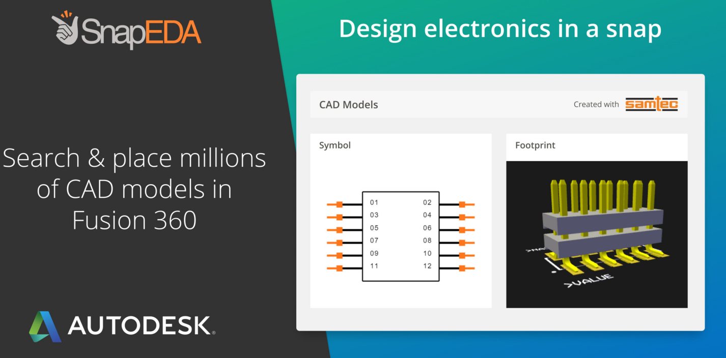
An integrated component library contains over 500k manufacturer parts covering all needs from single board hobby projects to complex professional hardware products development in verticals spanning IoT, robotics, industrial automation and consumer electronics.
This step-by-step walkthrough covers end-to-end electronics product development workflow from concept to manufacturing outputs leveraging SnapEDA’s schematic capture, simulation, PCB layout and co-design capabilities tailored for the hardware community.
Getting Started
To start your first design project, simply:
- Go to SnapEDA website
- Sign up for a free account
- Click Create Design button to initialize blank project
The integrated browser-based SnapEDA Editor will launch taking you into schematic capture mode ready to start placing components. Tutorial pop-ups provide interactive guidance introducing primary areas and functions.
Let’s begin the electronics design process!
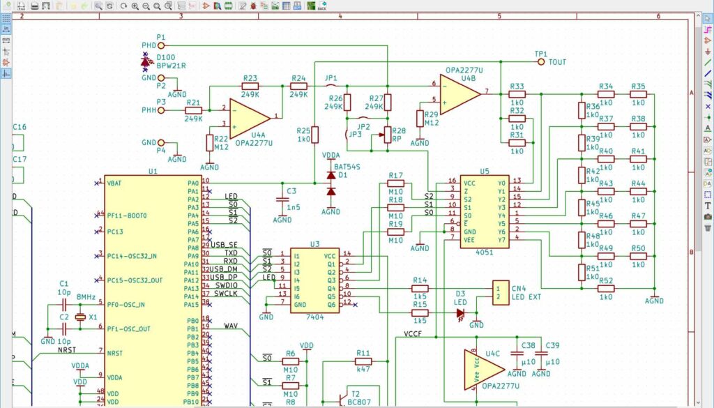
1. Schematic Capture

SnapEDA’s schematic editor provides traditional worksheet style canvas and wide range of drawing tools to create base schematics.
Below covers key concepts doing schematic entry:
Create Sheet
Grid buttons allow inserting A4 or Letter page sizes to start capture. Top toolbar shows page navigation between multiple sheets when design complexity builds up.
Add Components
From the left SnapEDA component browser showing 500k+ cataloged parts, select required devices and literally drag-drop symbols needed onto sheet. Repeat inserting parts until full bill-of-materials refines representing concept.
Draw Connectivity
Click wiring tool and trace connections between component pins to represent logical circuit connectivity flow. Visual cues indicate valid joins. Tap wire endpoints to cycle amongst available pin electrical types like input, output, passive etc.
Arrange and Annotate
Use alignment tools to neatly organize parts and wiresplaced. The Annotate button auto-sequences reference designators. Cross-probe highlighted nets between sheets using mouse overs.
Run Electrical Rules Check
Frequently validate connections integrity against missing pins and dangling wires using the built-in Electrical Rules Check (ERC). Fix reported issues incrementally as you build out complexity.
Add Details
Annotation tools allow documenting schematics with custom call outs, headings, error/warning markers and description boxes. Import images using drag and drop.
When ready, run final ERC to validate completion before saving prior to simulation or PCB layout conversion.
2. Simulation Setup
SnapEDA provides integrated circuit simulation capability to interactively verify logic operation right from within the Editor by placing probe pins, generating stimuli and inspecting node waveform behaviors to confirm functioning before committing expensive PCB prototype build cycles.
To setup simulation:
Attach Test Probes
From toolbar, choose Pin icons to drop Probe, Stimulus or GND pins onto nets needing inspection. Probes passively monitor signals, while Stimuli actively overrides to inject inputs.
Configure Simulation Models
For key ICs, right click instance to browse and attach simulation model to define behavioral logic. Standard model formats like Verilog, VHDL and SPICE supported.
For passives/discrete parts simulation abstraction auto-inferred from schematics.
Generate Stimulus
Click Stimulus pin and edit values waveform over time on popup. Define combinations to validate corner cases. Add more stimulus pins as needed to excite.
Run Simulation
The “lightning” icon triggers simulation solving. Probe pin waveforms display based on attached model logic and stimuli applied verifying operation before PCB layout routing.
Iteratively refine probes, models and stimuli while smoothly blending schematic design and simulation steps to finalize circuit performance meeting requirements using SnapEDA’s integrated electronics design environment.
3. PCB Layout
Upon schematics completion, click the PCB Layout icon to launch physical board layout canvas retaining all placed parts and connectivity.
Below outlines core concepts doing PCB layout within the SnapEDA editor:
Import Stackup
Start by defining layer count and materials. SnapEDA includes stackup templates for common fabrication processes and board types including FR4, Rigid-Flex, HDI and RF microwave.
Place Components
Parts from schematic get pre-imported ready for placement. Drag devices from left onto canvas and arrange based on grouping, size priority. Rotate and alignment aids assist interactive positioning.
Route Traces
Click Route Track to connect pads. Push and shove capability enables intelligent completion by dynamically nudging neighboring traces when dragging new connections through dense areas avoiding manual cleanup.
Validate Design Rule Checking
Set clearance rules and run Design Rule Checks (DRC) to validate spacing and constraints compliance between tracks/pads/vias. Errors highlight issues to address preserving manufacturability.
3D View and Emulation
Photorealistic 3D mode visualizes board and components providing mechanical fit verification through STEP export to external tools. Measure distance/clearance between objects directly by dimension lines. Pan, orbit and zoom controls aide inspection from all angles.
Copper Pour and Planes
Add copper pours/polygons for large fills tied to nets. The Auto-pour button automatically pours all remaining nets improving EMI control with entire area flooded. Split power and ground to separate polygons for isolation.
Output Manufacturing Files
When layout completes DRC clean, quickly generate industry standard CAM and documentation outputs including Gerber files, drill hits, assembly drawings, BOM and component placement centroid file for handoff.
Leverage SnapEDA’s unified EDA environment to smoothly link schematics into functional routed PCB layout ready for fabrication in minutes using cloud convenience from any OS without install headaches.
4. Co-Design and Team Collaboration

Once base design completes, leverage SnapEDA‘s real time collaboration features to securely interface with electronics manufacturing partners or ODMs through the cloud to streamline outsourcing production hand offs.
Below summarizes critical co-design capabilities improving supply chain interactivity:
Share Project Access
Under project settings, invite other SnapEDA users via email address to privately view or edit the design files in real time enabling distributed team cooperation reducing back and forths.
Comment and Annotate
Partners can place markers, annotations and comments on specific areas both on schematics and PCB layout layers needing attention improving clarity on potential DfM refinements needed without needing meetings.
Model Import
No EDA tool has all simulation models. Allow PCB partners to directly attach relevant IC behavior models under secured access improving model availability.
Engineering Change Order (ECO) Handoff
Managing iterations via ECO firmware is smoothed by graphical highlight tools to pinpoint redlines needed against latest PCB version accelerating identification of change point deltas.
By unifying design data access, communication and workflows between customer and suppliers within one platform, SnapEDA aims to bridge electronics hardware innovation barriers improving product development velocity from concept to certified production.
Final Files Export and PCB Ordering
Once design completes DRC verification through internal team review or external manufacturing partner inputs, export final data packs critical for procurement.
On editor top Toolbar, select Export Manufacturing Files containing:
- Gerber – Full layer plot files for board fabrication
- Drills – NC excelon drill hit table for machining
- Centroid – XY pick and place program for SMT assembly
- Drawings – PDF assembly drawings with callouts
- 3D Model – Mechanical STEP model for enclosure design fit
- BOM – Component list with supplier orderable part numbers
Upload zip bundle to your preferred PCB manufacturer quoting portal or sales rep inbox to kickstart fabrication and assembly.
Additionally share read-only version of SnapEDA design viewer link for any production partners to reference design intent without ability to edit.
And finally ordered boards delivered, leverage complementary SnapEDAParts mobile app to scan datamatrix codes on reels confirming exactly correct components getting mounted during SMT loading.
Thereby closing the loop from concept to validated production across the product development life cycle using SnapEDA’s seamless, cloud-based electronics design platform improving team productivity and manufacturing outcomes.
FAQs

What are the pros and cons of cloud-based EDA tool vs desktop?
Some benefits SnapEDA offers over traditional installable desktop EDA suites like Altium or KiCad include:
- Access designs from anywhere without needing software installed
- Real-time multi-user collaboration capability
- Frequent auto-updates with new features and fixes
- Standard login eliminates worry about data backups
However, some limitations versus powerful desktop applications are:
- Limited device model library without ability to run custom Spice simulations
- No native version control integration
- Restricted tool capability until features mature over time
- Requires stable internet connectivity when working
So evaluate specific use case priorities weighing convenience versus control when choosing between cloud-centric SnapEDA or unmatched power density from scriptable desktop EDA suites.
What file formats does SnapEDA support importing or exporting?
Below covers the standard interchange formats supported currently:
Schematics and Layout Import:
- Altium .SchDoc and .PcbDoc files
- KiCad .SCH and .KICAD_PCB files
- Eagle legacy .SCH and .BRD files
- DXF footprints
Export Output File Types:
- PDF schematics, assembly drawings and plots
- IDF 3D models
- CSV component lists
- Manufacturing Gerber and NC Drill files
- IPC2581 archival bundles
SnapEDA focuses OEM adaptor support on the most widely adopted community file formats from both proprietary and open-source Electronic Design Automation ecosystems through ongoing import/export capability expansion.
Can I get PCB prototypes assembled through SnapEDA?
Yes, SnapEDA offers in-house engineering grade PCB assembly service utilizing domestic US quick-turn assembly lines reducing lead times and enabling customer inspection during build process:
Assembly Capabilities
- SMT and Through Hole components
- 01005 passives to BGA packing
- Lead-free HASL and Immersion Silver finish
- Ultra fast 24 to 48 hour turnaround time
- Small batches starting 5 boards
Offering tight OEM integration between design, fabrication and assembly within one US-based company aims to accelerate proof of concept and prototyping during product development cycles through vertical expertise consolidation.
So bypass unpredictability outsourcing globally when requiring responsive, high mix/low volume complex board builds to verify SnapEDA Editor tool designed hardware.
I hope this full step-by-step guide gives electronics innovators and hardware teams confidence to take first concept ideas through successful routed layout and qualified assembled boards using SnapEDA’s intuitive yet capable cloud-based electronic design platform optimized smooth team collaboration.
With growing online component libraries access crossing 500k parts, deep quality fabrication networks assurance, and real-time commenting/transparency improvements, SnapEDA lowers barriers realizing advanced hardware products unmanned leveraging cloud convenience. Expedite your next IoT, robotics or smart device PCB project and experience the benefits through hands-on trial today!


