Ensuring the reliability of printed circuit boards over their target operating lifetimes demands rigorous test and analysis validation covering parameters like:
- Thermal stress endurance
- Vibration resistance
- Shock tolerance
- Environmental durability
- Electrical integrity
By exposing PCB system prototypes to a battery of characterized stress tests modeled on deployment conditions and collecting detailed performance data for review, engineers can reliably predict, improve and guarantee system lifespan milestones critical for end-use applications.
This guide surveys ten key PCB test and analytical validation to deploy when optimizing board reliability capabilities covering thermal, mechanical and electrical factors:
#1: HALT – Highly Accelerated Lifetime Testing

The Technique: HALT rapidly stresses boards with extreme temperature, vibration and voltage conditions until failures, determining design weaknesses.
The Purpose: Push PCBs far past realistic operating limits to uncover early life product flaws.
Application: Effective for improving PCB durability and lifespan by revealing correction opportunities targeting defects like solder joint cracking or capacitor desoldering that enable field issue avoidance.
#2: HASS – Highly Accelerated Stress Screening
The Technique: HASS utilizes high temp cycling, vibration and electrical loads to precipitate early product failures via stress screening.
The Purpose: Eliminate defective or damage-prone PCB assemblies by inducing test failures to identify units with latent flaws.
Application: When performed on manufactured PCB lots before shipment, failed test units confirming flawed boards can be discarded prior reaching field deployment for substantially enhanced quality and reliability.
#3: Aeromechanical Testing
The Technique: Aeromechanical testing analyzes PCB package structural responses when exposed to simulated dynamic airflows and pressures matching aircraft, vehicle and drone operating atmospheres.
The Purpose: Benchmark secured PCB’s abilities to withstand operating vibration levels caused by equipment systems like fans or mechanical linkages when integrated into target mobile platforms to determine needs for supplemental damping mounts or gaskets.
Application: Necessary to assess aerodynamic structural reliability of electronics payloads destined for aviation, defense or other high airflow transportation integrate roles.
#4: Shock and Drop Testing
The Technique: Shock machines hits PCB systems with high intensity low-duration impacts while drop tests assess effects of sudden hard contact with various associative orientations.
The Purpose: Validate shock mitigation and surrounding enclosure schemes used to protect boards and components from briefer spikes up to 1000+ Gs from occasional impacts.
Application: Particularly critical for portable electronics likely to suffer falls during mobile usage or systems traversing uneven terrain and experiencing sharp transient bump loads above typical smooth vibration ranges.
#5: Mixed Flow Testing
The Technique: Combined environments boxes expose PCB assemblies simultaneously to multiple stressors like temperature extremes ranging from -100°C to 260°C, 95%+ humidity, vibration levels mimicking rotary wing aircraft along with electrical loads nearing maximum capacity ratings.
The Purpose: Confirm PCBs collective robustness when facing concurrent environmental, mechanical and electrical threats replicating intensely punishing installation environments instead of testing solely along single parameter axes.
Application: Mission-critical structural electronics operating in highly dynamic mechanically stressful external conditions where multidimensional threats abound.
#6: Hermetic Seal Testing
The Technique: Hermeticity testers check sensitive PCB component vacuum seals for leakage integrity using test methods like optical detections or pressurized helium mass-spectrometry to precisely determine leakage rates.
The Purpose: Validate sealed protective enclosures fully isolate internal PCB environments from external contamination ensuring stable interior conditions over product lifetime along with analytical forecasting of future leakage risks.
Application: Necessary quality control confirmation for electronics containing micro-electromechanical systems in aircraft and spacecraft applications where air pressure differentials risk vacuumed container integrity.
#7: Burn-In Testing

The Technique: Burn-in testing runs boards at elevated temperatures and voltages for prolonged intervals spanning days to precipitate latent early-life electronic component failures from manufacturing defects.
The Purpose: Improve quality by eliminating damaged boards and unstable premature parts before deployment. Confirm design margin allowances agree with application lifetime projections at sustained edge ratings.
Application: Effective for enhancing reliability of boards supporting critical infrastructure or military systems undergoing little servicing where high confidence in electronics stability spanning a decade or longer proves paramount.
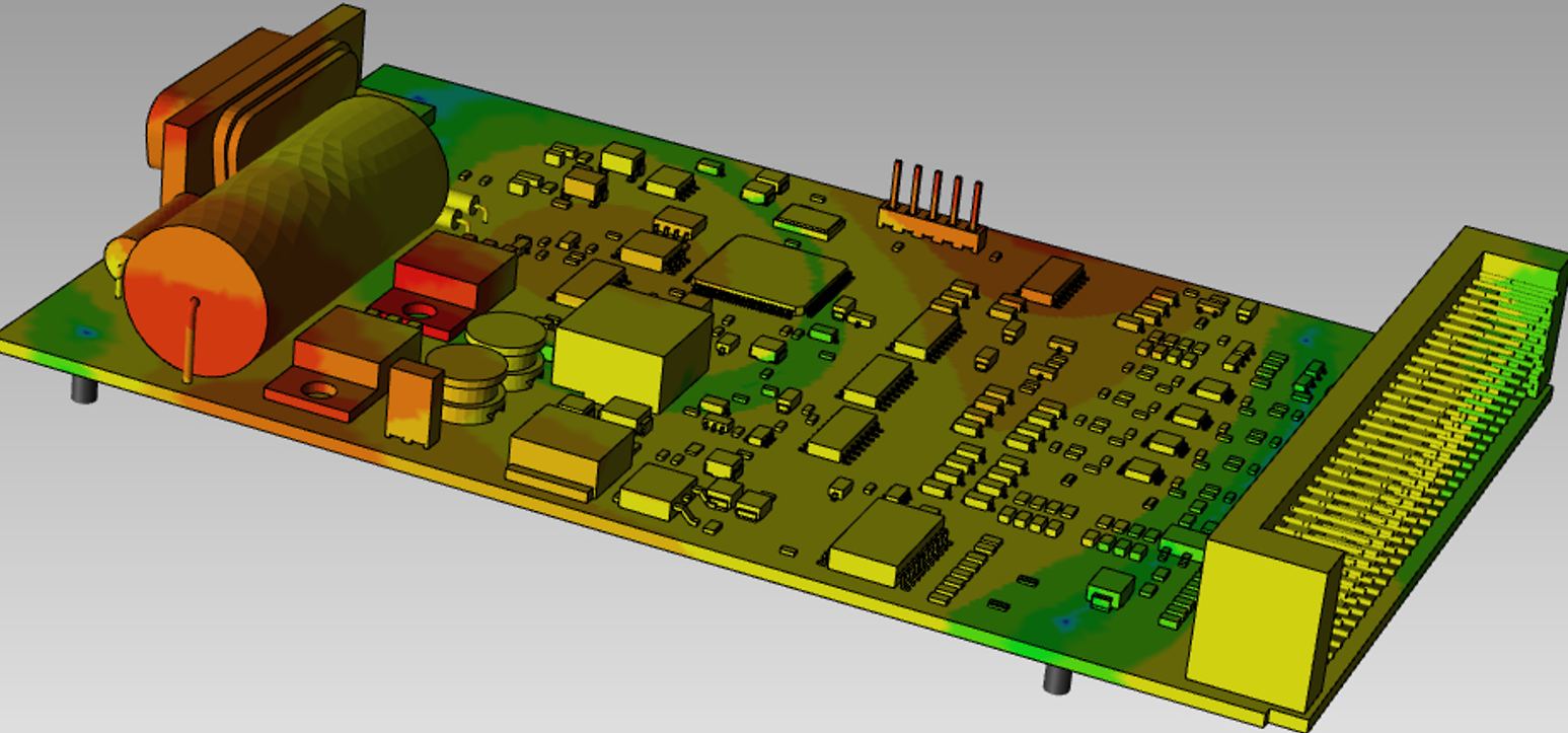
#8: Signal Integrity Testing
The Technique: Signal integrity testing utilizes specialized instrumentation and simulation to model interconnect performance across entire PCB systems capturing timing, reflections, EMI and other behaviors at high frequencies.
The Purpose: Ensure complex multilayer boards with dense components operate reliably meeting speed necessities across traces, vias and interfaces for high-speed applications without analog signal degradations degrading noise margins.
Application: Mission critical PCBs handling fast multi-gigabit data rates with tight timing margins like servers and network infrastructure gear demand signal integrity validation ensuring robust error-free operation over long operating lives before manufacturing ramp.
#9: Thermal Endurance Testing
The Technique: Thermal endurance testing allows measuring degradation effects on solder joint crack propagation along with thermomechanical stress impacts on BGA interfaces when boards undergo repeated aggressive temperature spike and soak profiles from -65°C to 150°C for assessing lifetime expectancy given deployment conditions.
The Purpose: Confirm solder joint fatigue models match intended reliability targets like 1000 cycles spanning 0-100°C determining number of high temp excursions boards can withstand during usage meeting milestones like 10 year lifetime projections.
Application: Particularly relevant for outdoor telecom/5G gear and automotive electronics expected to experience substantial environmental swings informing design margins, heating, cooling and enclosure choices boosting reliability.
#10: Field Testing
The Technique: Field testing deploys functional PCB systems into factual target environments paired with remote monitoring allowing capture of performance data over months and years.
The Purpose: Despite best lab testing efforts, real world conditions invariably differ from models eventually revealing failure points only observable from long term installations. Field testing tackles the enormous challenge of confirming highly reliable electronics both survive and perform up to expectations when facing messy actual stimuli.
Application: Field testing marks the final validation hurdle conferring highest reliability status to productized boards destined for critical infrastructure and remote deployments where frequent maintenance access proves impractical.
In summary, by progressing PCB systems through a progression of testing complexities in concert with simulation models and teardowns, engineers can methodically refine designs targeting stability milestones like 10 or 20 year lifespans even for electronics facing extreme mechanical and environmental stresses over their tenure. Careful test design, diligent result interpretation and insightful design responses that avoid over engineering enables striking optimal reliability and cost balances.
Frequently Asked PCB Reliability Testing Questions

What are the 3 key factors influencing PCB reliability?
Thermal cycling, mechanical shock/vibrations and electrical stresses represent the prime factors degrading PCB integrity and longevity through mechanisms like metal fatigue, fractured traces or solder joint cracking ultimately triggering field failures.
Which test is used to determine PCB reliability lifetime?
While HALT, HASS and burn-in accelerate infant mortality screening, thermal endurance cycling provides the most direct measurable test method for projecting future PCB reliability lifetimes based on quantified solder joint thermal fatigue responses used to extrapolate operate cycle survival estimates.
What is the difference between HALT and HASS testing?
HALT aims to break products revealing design weaknesses for improvements, while HASS seeks to uncover damaged units with latent flaws normally escaping standard testing for removal prior to field deployment via aggressive stress screening.
How long does it take to test PCB reliability?
Rigorously qualifying PCB lifetime reliability necessitates months to years of testing iterations spanning thermal cycling, vibration, electrically loading along with simulation correlations to fully characterize design margins and risks – but delivers associated confidence in application robustness.
What are the 5 key environmental tests for PCBs?
Temperature cycling, mixed flowing gas exposures, humidity-freeze, mechanical shock/vibration and visual inspection represent the prime environmental tests per IPC standards to qualify PCB robustness for deployment into challenging real world settings.


