Rapid printed circuit board (PCB) prototyping involves iteratively building quick test boards early when developing new electronic products. Leveraging faster design-to-fabrication workflows minimizes costly design mistakes before high volume manufacturing by validating electronic hardware operation early alongside enclosure fit assessments. This guide covers planning considerations, comparing prototyping approaches, ideal design principles and reviewing results when getting custom PCB prototypes built rapidly to accelerate overall development timelines through reduced respins.
Setting Rapid PCB Prototype Goals
Start by defining what specific issues need evaluating by quick-turn test boards differencing prototyping builds vs final mass production run.
Key Validation Areas
- Circuit integrity under power
- Fault finding shorts/opens
- Refining breadboardconstructs
- Firmware compatibility testing
- Early RF/analog signal verifications
- Mechanical fit check
- Design rule checks discoveries
Balancing Tradeoffs
Prototyping faster does trade off some fidelity checks reserved for full fabrication like rigorous specifications on:
- Layer counts
- Finer trace/space widths
- Temp fluctuation resistance
- Vibration resilience
- Environmental sealing
- Compliance approvals
But fast prototype boards quickly assess primary functionality, dimensions and basic performance metrics.
Comparing Approaches for PCB Prototypes
In-House Milling
Manually carving board substrates using desktop CNC mills provides fully customizable results with little startup costs beyond equipment but requires learning mastering mechanical techniques alongside dealing with material limitations and precision challenges.
Best for simple single-sided hobbyist PCBs.
DIY Chemical Etching
Chemically corroding copper laminates with printed toner transfers allows adequately featured PCBs relying on additional post-etch processing like drilling and plating but can risk over-etching causing track widths falling out of tolerance.
Convenient for custom single-sided boards.
Batch Assembly Services
Sending Gerber artwork to budget board houses in China can produce quality basic 2+ layer boards affordably, however, costs advantages trade off 4+ week lead times unsuitable for rapid iteration during development.
Low-cost option once design finalize.
Specialized Proto Houses
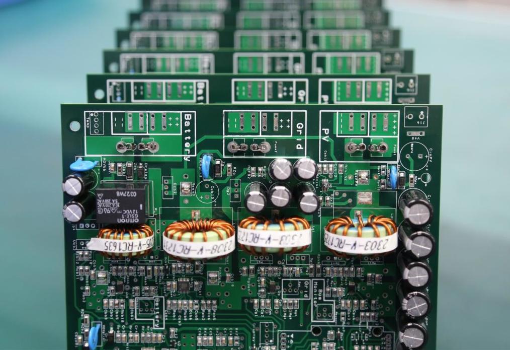
Dedicated quick-turn prototype shops leverage automated expert workflows minimizing handling utilizing advanced manufacturing equipment so designers receive boards in just 1-5 days allowing rapid testing feedback benefiting optimization efforts prior to final release builds.
The preferred solution for rapid prototyping.
Ideal Design Rules for Prototype PCBs
Balancing complexity to validate core functionality while minimizing unique footprint libraries, BOMs lines and advanced stackups during prototyping maximizes fabrication feasibility and cost control:
Pick Widely Available Components
Sticking to common 0805 or 0603 Imperial size surface mount packages along with SOIC through-hole ICs reduces chances of unavailability issues delaying orders since most assembly shops stock these universally.
Utilize 01005 Packages Cautiously
When needing tiny footprint planted components like 0201/01005 imperial sizes, avoid arrays exceeding at least 20+ units per placement allowing sufficient pick and place vacuum nozzle sampling areas else risk assembly difficulties driving up prototyping costs unnecessarily.
Favor 2 Layer Boards
Keep conductive layers to 2 when possible since adding extra layers grows costs exponentially due to requirements around alignment, registration, lamination while not likely providing substantial benefits for early testing needs thus preserve budget for extra iterations.
Prioritize Top and Bottom Layers
Reserve inner buried layers only for dense high pin count BGA footprints unavoidable in prototypes else maximize routing across readily accessible top and bottom sides enabling easier debugging later under magnification.
Allow Sufficient Clearances
While final product may utilize tighter manufacturing tolerances, prototype PCBs should stick to 1oz copper weights with at least 5 mil spacing and traces no thinner than 6 mils to prevent potential shorts causing assembly failures before full debug testability achieved.
Table comparing ideal prototyping vs production design rules | Specification | Prototype | Production | |---------------|-------------|-------------| | Trace Width | > 6mil | > 3mil | | Trace Spacing | > 5mil | > 3mil | | Copper Weight | 1oz | 2oz |
Ensuring DFM Practices
Several critical design-for-manufacturability guidelines must get followed when submitting prototypes focusing on maximizing fabrication and assembly success rates:
Provide Complete Gerbers
Always supply a full set ofGerber files detailing silkscreen, solder mask, copper layers, drill drawings, netlists, etc rather than assuming PCB vendor will figure out undisclosed design elements since lack of clarity risks misinterpretations that impede outcomes.
Avoid Teardrops Sparingly
Some CAD tools automatically inject rounded teardrops at trace junctions preventing etchant seeping beneath thin copper that causes unwanted opens. However, excess teardowns interfere depotting during rework so apply only moderately at few selective sharp junctions when prototyping to enable better editing later allowing test point access.
Request Lead-Free HASL Finish
Specify lead-free HASL surface finish ending up economical while avoiding regulatory issues that could delay border clearances associated with lead tinning options during rapid iteration stages. Importantly, lead-free solders still fuse components adequately during profiling allowing validation before final ENIG gold immersion of production runs.
Outline Panel Utilization
Detail expected board outlines aligned efficiently within panel areas optimizing mechanical fabrication tolerances while accommodating available substrate sizes to prevent additional tooling fees getting passed due to shifts after prototyping gerbers sent.
Confirm Hole Sizes
Double check hole diameters get drawn 1-2 mils larger than drill bit widths listed in accompanying fabrication notes for prototypes allowing slight registration misalignments given faster tooling processes that would cause costly broken drill bits if tight clearances tried matching full production runs too soon. This prevents avoidable handling delays for small batches.
Reviewing Rapid Prototype PCB Results
Once boards get delivered, inspect carefully at each assembly stage:
Prep Components
Before population, examine PCB finish under magnification checking for potential gaps around traces, inconsistent wetting or missing openings that could impede soldering or probe testing points later.
Solder Carefully
Follow manufacturer recommended thermal profiles with adequate ramp up, peak and cool down stages allowing sufficient reflow while preventing thermal shock that cracks boards requiring reworks.
Confirm Alignment
After soldering, scan boards oriented both horizontally and vertically under high zoom verifying component alignments stay within specified coplanar tolerances using same processes as final SMT lines would for enhancing future transition smoothness.
Functionally Test
Upon electrical validation, stress test prototype boards through repeated hot cold cycling, regulating supply voltages across operating ranges and monitoring functionality at extremes as indicators of hardware capability covering limitations that finalized production testing would reveal.
Assess Optimizations
Log any estimation inaccuracies, performance restrictions or enhancement opportunities to upgrade next revision.
Carefully vetting interim fast-turn prototypes uncovers tangible issues early preventing extensive mid/late-stage redesigns ultimately accelerating overall development pace towards stable final release.
Questions and Answers
Q: Can PCB prototypes get functionally tested before soldering components?
A: Yes, using flying probe testers, unpopulated boards undergo electrical validation through points sampled digitally across various nets checking for potential opens or shorts between nodes that could get missed under post-assembly visual inspections alone highlighting need for design tweaks.
Q: What are practical ways to lower costs when prototyping complex boards?
A: Substituting rigid or flex-rigid PCB materials for cheaper FR-4 grades yet retaining similar stackup arrangements during prototyping combined with specifying cheaper immersion silver finishes instead of gold reduces expenditure while still validating primary functions just fine before final ENIG production boards.
Q: How can prototyping costs get cut when working with 4+ layer count boards?
A: During prototyping, rather than fabricating all layers symmetrically, removing few mid layers replacing with jump wires grants inspection access from top layer while retaining primary power delivery and ground planes essential for basic testing thereby lowering expenses.
Q: What steps can be taken if prototypes get delayed at board houses?
A: To accelerate prototyping, designers can assist vendors by ensuring Gerber files already setup for panel utilization avoid unnecessary tooling rework alongside requesting simpler 1oz builds foregoing heavy copper if timing pressures arise. Finally, relaxing interim spacing/trace rules preventing respins unblocks processes.
Q: Why do certain prototype PCBs costs exponentially more than others?
A: Significantly higher prototype expenses arise from incorporation of thicker copper weights for high current carrying needs, addition of extra prepreg/core layers essential for impedance tolerances or utilization of expensive RF laminates mandatory for regimented dielectric constants hitting target performance which all get mandatory for production thus increasing piece part costs.
Conclusion
In summary, rigorously planning PCB prototyping manufacturing leveraging preferred design guidelines enables testing form-factor fits, electrical connectivity nuances and performance characterizations rapidly receiving feedback over short time spans. This allows engineering teams to incrementally improve subsequent revisions systematically de-risking discoveries earlier ultimately speeding end products development greatly minimizing costly overruns and delays afterwards.


