
Introduction
High-density interconnect (HDI) PCBs refer to boards with very dense conductor patterns and interconnects achieved through microvia technology. They allow integrating complex ICs with high pin counts and shrinking product form factors.
Compared to standard PCBs, HDI boards offer miniaturization, performance enhancements, and design flexibility. However, the fabrication process is also more intricate. This article provides a detailed overview of HDI PCB technology, manufacturing methods, design considerations, applications, advantages and limitations.
The key enablers of HDI boards are:
- Extremely fine lines and spaces
- Smaller vias and capture pads
- Thinner dielectric layers
- Sequential lamination
- Microvias for layer interconnections
By employing these in optimized stackups, interconnect densities exceeding 20,000 I/O per square foot can be realized. Let us look at each of these HDI technology elements and the complete manufacturing process flow.
HDI Design Rules
HDI boards follow tighter design specifications:
Trace and Space
- Line width/space: 25μm (1 mil) and under
- Commonly 2-6 mil lines/spaces
Via Sizes
- Microvias: Below 150μm diameter (6 mil)
- Common sizes 25μm to 125μm
Dielectric Layers
- Thinner laminate and bond ply layers: 25μm to 50μm
Stackup
- Typically between 4-8 layers
- Some high performance boards up to 20 layers
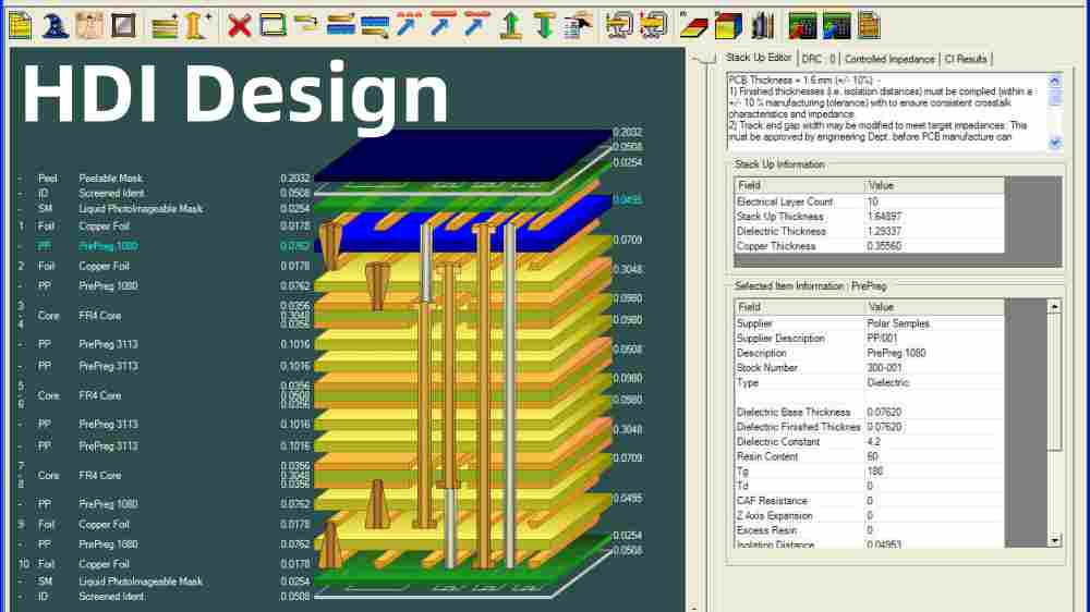
HDI Layer Stackup Configuration
A typical HDI board stackup contains:
- Inner microvia layers
- Outer conventional layers
- Buried and blind vias
- Thin core and prepregs
For example:
- Top and bottom layers with wide traces and pads.
- Thin core and prepreg layers.
- Dense microvia layers connected using sequential lamination.
- Mixture of buried, blind and through vias.
This optimized arrangement locates the dense routing layers internally, minimizing via lengths.
HDI Manufacturing Process Steps
Specialized fabrication techniques are required to manufacture multilayer HDI boards:
1. Inner Layer Formation
- Build up inner HDI layers with microvia interconnects.
- Use thin dielectric cores (25-50 μm) and bond plys.
- Construct 2 or 4 layer core with microvia interconnects.
- Laser drill microvias (25-150 μm diameter).
2. Outer Layer Fabrication
- Fabricate conventional outer layers separately.
- Apply required routing, solder mask, silkscreen.
- Drill outer layer vias before lamination.
3. Sequential Lamination
- Align and laminate HDI and outer sub-assemblies.
- Use heat, pressure and resin flow to bond stackup.
- Fill gaps and encapsulate layers.
4. Via Formation
- Use laser and mechanical drilling for microvias and through holes.
- Plate copper to fill holes and form interconnections.
5. Patterning and Finishing
- Define traces on outer layers by lithography and etching.
- Apply solder mask, legend, coatings.
6. Singulation
- Rout individual boards from panelized assembly.
7. Electrical Testing
- Test connectivity, insulation and functionality.
HDI Microvias

Microvias create connections between layers in HDI boards:
Types
- Blind Vias – Connect inner layers, capped by outer layer
- Buried Vias – Only connect inner layers
- Through Vias – Span entire board thickness
Sizes
- High density microvias are below 150 μm (6 mil)
- Conventional vias are over 250 μm
Geometries
- Circular is most common
- Elliptical and rectangular also possible
Fabrication
- Laser drilling provides small via capability
- Precise depth control to avoid hitting inner layers
- Minimal clearance needed around vias
Microvias enable routing escape paths from dense BGA packages while minimizing via lengths for optimal high frequency performance.
HDI Design Considerations
HDI technology impacts PCB layout:
- Account for HDI constraints like line width, spacing, via sizes upfront.
- Leverage microvias to route out of tight spaces.
- Utilize diagonal routing with 45° traces.
- Plan ahead for hot spots and heat dissipation from tightly packed components.
- Watch out for acid traps during etching to avoid unwanted openings.
- Minimize unused areas which increase risk of shorts and etching variation.
- Guard against glass fibers wicking resin during lamination and causing microvia voids.
- Allow sufficient capture pad clearances around microvias.
- Incorporate thermal relief connections for surface mount devices.
- Review layouts, stackup and outputs thoroughly – rework is very difficult.
Careful HDI board design is key to avoiding manufacturability issues and gaining maximum benefit from the density capabilities.
HDI PCB Applications
Some major application areas include:
Consumer Electronics
- Smartphones, tablets, laptops
- Wearables, hearables, smartwatches
- Drones, robots, IoT devices
Telecom/Datacom
- Networking cards and switchboards
- Data storage products
- High speed computing
Medical
- Implants, monitors
- Ultrasound transducers
- Imaging systems
Automotive
- Engine control units
- ADAS systems
- Infotainment and telematics
Aerospace/Defense
- Avionics electronics
- Satellite payloads
- Radar and communication
HDI PCB Advantages
Key benefits of HDI PCB technology include:
Miniaturization
- Microvias allow escape routing from fine pitch components
- Thin dielectrics reduce space between layers
- Enables smaller and lighter end products
Higher Density
- Accommodate more I/O connections
- Integrate components compactly
- Maximize board real estate
Improved Electrical Performance
- Faster speed with tightly spaced traces and ground planes
- Shorter via interconnects
- Controlled impedances
Design Flexibility
- Route out of tight spaces
- Access inner layers directly using microvias
- Embed components or circuits
Reliability
- Thick copper outer layers and solid power/ground planes
- Good thermal performance
- Withstand shock, vibration, drops
HDI PCB Limitations
There are also some limitations to consider:
Fabrication Complexity
- Tight process controls needed for thin dielectric layers
- Precise laser drilling and hole plating
- Higher rejection rates and cost
Design Overhead
- Meeting stackup, trace width and via size rules
- Ensuring manufacturability, testability and repair
- Extensive review to avoid re-spins
Limited Board Size
- Challenging to scale above 20”x 24” sizes
- High press pressures during lamination
Thermal Issues
- Hot spots from dense components
- Limited heat spreading paths
Testing Difficulties
- Accessing inner layer signals for bed of nails testing
- Fixtureless in-circuit testing preferred
HDI Fabrication Capability and Cost Trends

Technology Trends
- Laser via drilling down to 25μm
- 15μm line/space capability
- 5-10 layer stackups (more with thicker cores)
- Improved sequential lamination process control
Volume and Cost Trends
| Year | HDI Volume Share | Cost vs. Standard PCB |
|---|---|---|
| 2000 | <5% | 4X cost |
| 2010 | 15-20% | 2X cost |
| 2020 | 25-30% | 1.5X cost |
- HDI volumes slowly increasing with user adoption
- Technology maturation bringing down cost premium
- Still 1.5 to 2X cost verses standard PCBs
Conclusion
In summary, HDI provides a powerful technology to achieve highly compact and integrated PCBs by incorporating sequential lamination, thin dielectrics, microvias, and fine geometries. This enables next-generation electronics with space and weight savings. However, HDI also involves tighter design rules, fabrication complexity, performance considerations and higher costs that must be strategically managed. As the technology continues progressing, HDI usage is expected to accelerate for space-constrained portable and wearable products.
HDI PCB FAQs
Q: At what layer count does it make sense to choose HDI instead of a conventional PCB?
A: Typically 6 layers and above is where HDI value emerges – microvias and sequential lamination avoid the need to route very long traces. Below 6 layers, conventional PCB capability may suffice for many designs.
Q: How common are microvia failures and how can they be prevented?
A: With careful process control, microvia failure rates are under 5%. Voids can be minimized by validating drill parameters, etchback on pads, glass fiber resin wicking prevention, and thermal relief connections.
Q: How are components attached to HDI boards?
A: SMT components are commonly used with microvias allowing escape routing from fine pitch ICs and BGAs. Large pads, solder or conductive epoxy may be used for attaching connectors or sockets.
Q: What are some key tests performed to qualify HDI boards?
A: ICT and flying probe testing validates electrical connectivity. Micro-sectioning and microscopy inspects microvia structural integrity and layer bonding. Environmental stress testing verifies robustness.
Q: How repairable are HDI PCBs?
A: Repair is extremely challenging – limited access to inner layers and microvias with very fine geometries. Focused design strategies should ensure testability, but overall scrap and rework rates are higher for HDI boards.


